Streamlining Memory Reliability Testing for Faster, Smarter Data Storage Solutions
Invented by KANG; Youngsan, KIM; Donghee, LEE; Unho, JUNG; Jungho, CHOI; Jongkyu, Samsung Electronics Co., Ltd.
Welcome! Today, we’re going to talk about a new patent application that introduces a better way to test memory systems, like the memory chips inside your computer or phone. We’ll break down the patent into simple ideas and walk you through why this matters, how it builds on older technology, and what makes this invention unique. Let’s get started.
Background and Market Context
To understand this patent, it’s helpful to know how memory systems work and why testing them is so important. Nearly every device, from laptops to gaming consoles, uses memory chips (like DRAM) to store and move data quickly. These chips need to be very reliable because even a small mistake can crash software, corrupt files, or slow down performance.
Manufacturers and engineers test memory chips at different stages: when they are built in factories, when they are put into computers, and even while they are running. They want to make sure that data can be written (stored) and read (retrieved) without any errors. But here’s the tricky part: when a test fails, it’s often hard to tell if the problem happened while writing or reading the data. This confusion can slow down repairs, make troubleshooting harder, and even hide bigger issues.
The tech industry has been searching for ways to make memory testing faster, more accurate, and less confusing. This is especially important as chips get smaller and faster, and as we rely more on cloud computing, artificial intelligence, and other data-heavy tasks. In big server farms or in safety-critical systems like cars and airplanes, a memory error can have serious consequences.
Today’s memory tests can take a long time and may not always pinpoint the exact problem. Some older methods need data to be sent back and forth many times, which wastes time and power. As devices get more complex, the need for smarter, faster, and more precise memory testing has never been greater. This is the market context where the new patent steps in.
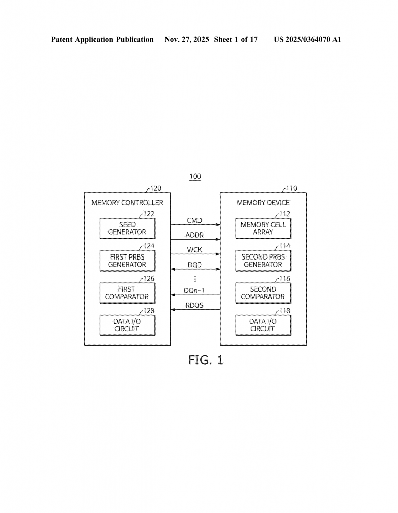
The patent we’re exploring introduces a method that allows both the controller (the “brain” that manages memory) and the memory chip to work together using a special kind of random number called a pseudo-random binary sequence (PRBS). By sharing a single starting number (called a seed), both sides can create the same sequence of numbers, which they then use to test the memory. This approach makes testing more reliable, faster, and can help engineers quickly figure out if a problem is with writing or reading data.
With the need for better memory testing tools only increasing, this patent could help manufacturers cut costs, improve quality, and make devices more trustworthy for everyone.
Scientific Rationale and Prior Art
Let’s take a look at the science behind this invention and how it compares to what came before. Memory testing isn’t new. For many years, engineers have used patterns of data—like all zeros, all ones, or repeating numbers—to check if memory chips are behaving correctly.
But using simple patterns has its limits. They might not catch every kind of error, especially in high-speed chips. That’s why engineers started using PRBS, which stands for pseudo-random binary sequence. Think of PRBS as a long line of numbers that looks random but is actually created by a mathematical formula. If you start with the same seed (a starting value), you always get the same sequence. This is very useful for testing because both sides can know what to expect without needing to send the whole pattern over.
Traditionally, PRBS testing in memory systems worked like this: a test device generates a PRBS, sends it to the memory chip, and then reads it back. If what comes back matches what was sent, the test passes. If not, there’s an error. But, if an error pops up, it can be tough to know if the trouble was with writing the PRBS, reading it back, or something in between.
Older patents and designs tried to solve this by adding extra steps, like sending the data again, using error correction codes, or having lots of extra circuitry to track problems. Some systems would require the data to be sent multiple times to make sure there were no mistakes. Others would lock in certain testing patterns, making them less flexible for different types of memory or different manufacturers’ chips.
And then there’s the issue of compatibility. Not all memory chips or controllers are made the same way. Some use slightly different ways to create PRBS (for example, different types of linear feedback shift registers, or LFSRs, which are like little math engines inside the chip). If the controller and the chip don’t agree on which LFSR to use, or how long the PRBS should be, their test patterns won’t match, making tests useless.
The new patent builds on these older ideas but solves several key problems:
First, it lets both the controller and the chip share a seed and agree on the type and length of the PRBS, so they can always generate the same sequence, no matter who made the chip or controller. Second, it allows each side to test the data independently and even at the same time—so if there’s a problem, it’s much easier to tell if it happened during writing or reading. Third, it allows results to be stored and shared in a special register (like a notepad inside the chip) so the controller can check what happened, even after the test is done.
By allowing flexible PRBS types, supporting chips from different makers, and making it easy to tell where errors come from, this patent takes memory testing a big step forward compared to the prior art. It’s a smart blend of old and new science, applied in a way that solves real-world problems.
Invention Description and Key Innovations
Now, let’s dive into what this patent actually describes and what makes it special. At its core, the invention is about a memory system that uses PRBS for testing, but with several clever improvements.
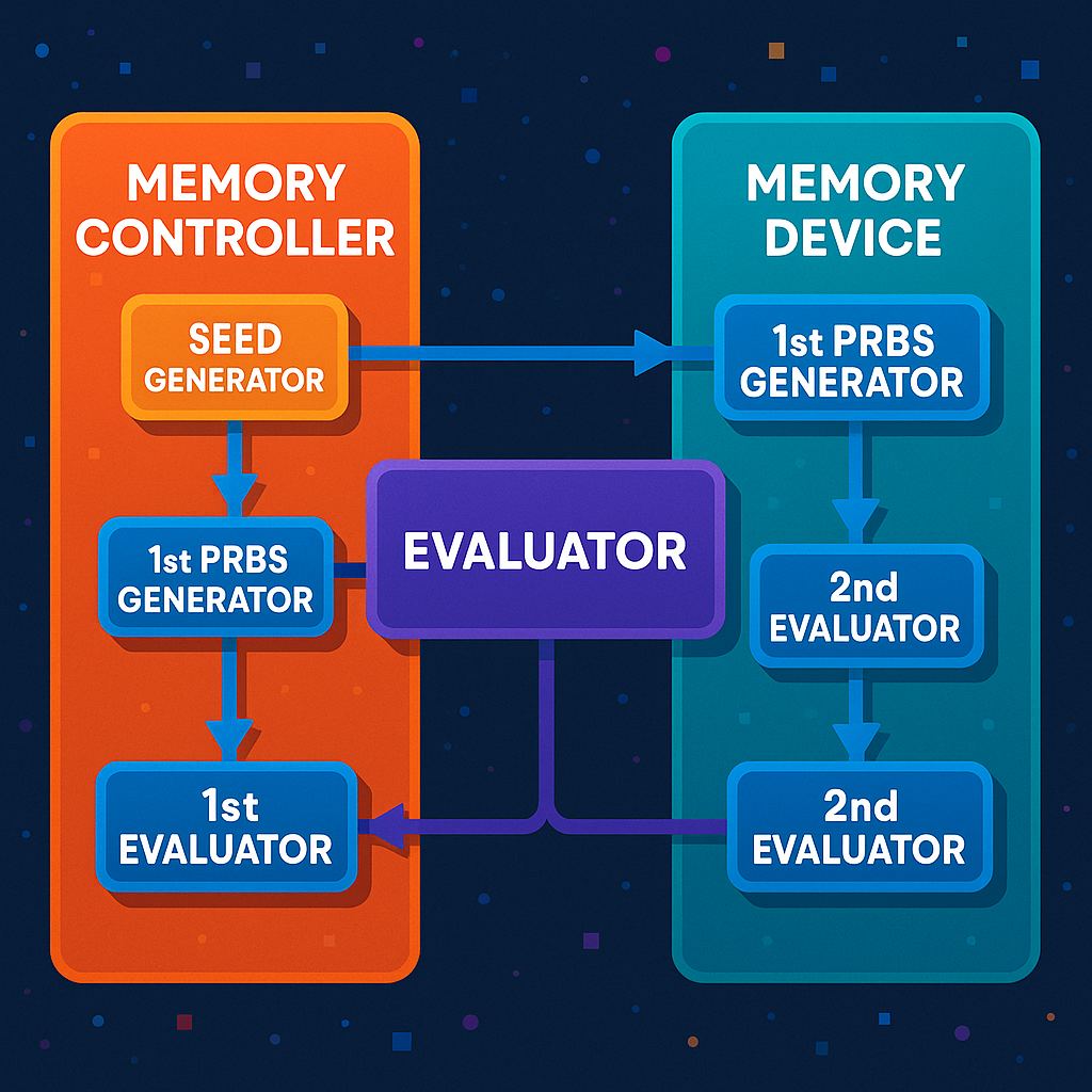
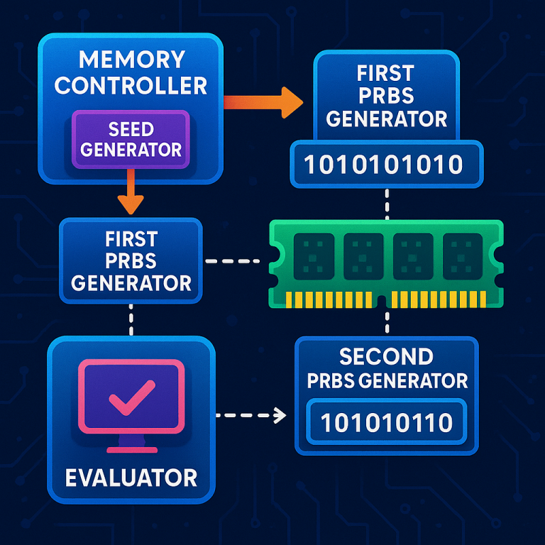
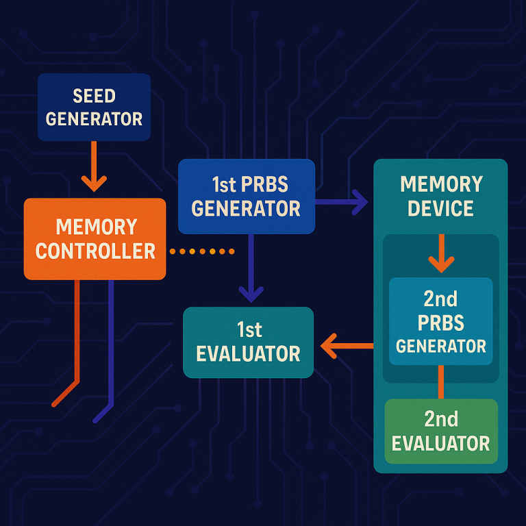
The system has two main players: the memory controller and the memory device (the chip). Both of them have their own PRBS generators. These are small circuits that, when given the same seed, will spit out the same sequence of numbers. This is like giving two people the same recipe and ingredients—they’ll cook the same dish.
Here’s how the process works:
First, the memory controller creates a seed value. This is a special number, and it’s sent to the memory chip. Both the controller and the chip use this seed to start their PRBS generators. But before this happens, the controller checks with the chip to see what type of PRBS generator (LFSR type) and what length it supports. This means the controller and the chip can always use a matching recipe, even if they were made by different companies.
Next, both sides generate their PRBS—a long string of numbers that looks random but isn’t. Depending on the test being run, the controller or the chip acts as the evaluator. If we’re testing how well the chip can be written to, the chip compares what it receives to what it generates, and stores the result. If we’re testing how well the chip can be read from, the controller makes the comparison.
One of the key innovations here is flexibility. The controller can ask the chip which kinds of PRBS it supports (for example, Galois or Fibonacci types of LFSR), and how long the sequences can be. This means the same controller can work with lots of different chips, and vice versa. No more being locked into a single method.
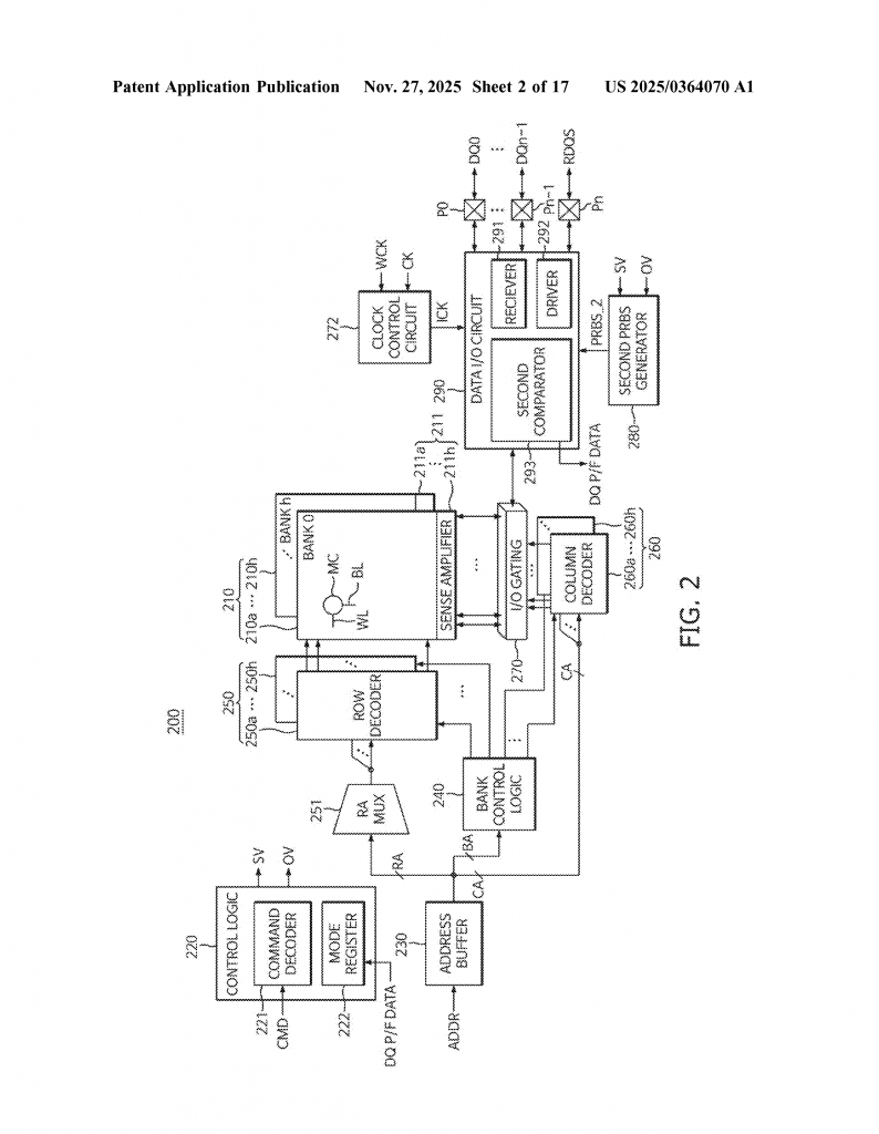
Another big improvement is how results are handled. The chip has a special register (like a digital notebook) where it stores the result of the write test. The controller can then read these results later, making it easy to see which data lines passed or failed. This is especially useful when testing many lines at once, which is common in modern memory systems.
The patent also describes how each data line (the wires or paths that carry data between controller and chip) can be tested separately or together. This makes it possible to find exactly which line has a problem, instead of just knowing that “something’s wrong.” The system can even run different PRBS on different lines at the same time, making tests faster and more thorough.
Another smart feature is the ability to use the same seed and PRBS setup for repeated tests, like in Shmoo testing. This is when you test the chip under lots of different conditions (like different temperatures or voltages) to see how it behaves. The system can quickly run these tests over and over, changing just the conditions, and easily compare results.
Here are some other highlights of the invention:
– The controller and chip can share not just the seed, but also “connection coefficients,” which are like special settings for the PRBS generator. This makes sure they always match.
– The system can send and receive PRBS data on multiple lines at once, and check each one separately.
– The results for each line are stored individually, so if only one line has a problem, it won’t be missed.
– The controller can ask the chip for its test results anytime, making troubleshooting and repair easier.
– The whole process can be used in different types of memory systems, not just DRAM, and in all sorts of devices from computers to cars.
What makes this invention truly special is how it brings together flexibility, speed, and precision. By allowing both sides to agree on how the test works, and by making it easy to see exactly where problems are, it helps manufacturers build better, more reliable devices. It also saves time and money, since fewer tests need to be repeated, and problems can be found and fixed faster.
In a world where memory reliability is more important than ever, this invention gives engineers a powerful new tool. It’s a smart, simple idea—let both sides create the same test pattern using a shared seed, and let each side check the results in real-time, storing them for later review. This approach means better quality, faster production, and more confidence for everyone using digital devices.
Conclusion
The patent application we’ve explored today brings a much-needed upgrade to the way memory systems are tested. By using shared seeds and flexible PRBS generation, it allows memory controllers and chips to work together smoothly, no matter who built them. This makes tests faster, more accurate, and easier to understand—helping engineers quickly pinpoint problems and fix them before they reach the end user.
This new approach is a big step forward for the tech industry, offering a way to make memory devices more reliable and efficient. As our reliance on digital devices grows, innovations like this will continue to play a crucial role in keeping our computers, phones, and other gadgets running smoothly. If you’re involved in memory design, testing, or manufacturing, this is a patent to keep your eye on, as it could soon set the standard for how memory testing is done worldwide.
Click here https://ppubs.uspto.gov/pubwebapp/ and search 20250364070.