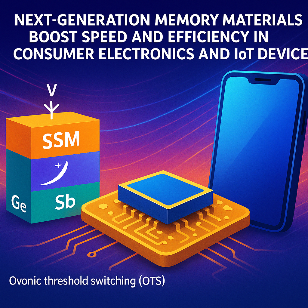
Next-Generation Memory Materials Boost Speed and Efficiency in Consumer Electronics and IoT Devices
Invented by YANG; Kiyeon, SUNG; Hajun, KANG; Youngjae, LEE; Changseung, Samsung Electronics Co., Ltd.

Modern electronics are getting smaller, faster, and smarter, driving a huge need for better memory devices. A recent patent application introduces a new type of memory material and device that could change how data is stored in phones, computers, and even artificial intelligence systems. This article will help you understand what makes this invention special, why it matters, and how it fits into the world of technology today.
Background and Market Context
Today, we live in a world filled with digital gadgets. Phones, laptops, and smart devices rely on tiny memory chips to remember everything from photos to messages. As these devices get thinner and more powerful, the demand for tiny, efficient, and reliable memory keeps growing. Traditional memory chips have reached their limits in size and speed, so the tech industry is always searching for new ways to store more data in smaller spaces.
Older memory technologies need two main parts inside each cell: one part to store the data and another part to control which cell gets read or written. This setup uses more space and power. To make memory devices smaller and more effective, engineers want to combine these two parts into one. This is where self-selecting memory (SSM) comes in. SSM can both store data and control access, all within a single device. That means simpler designs, smaller chips, and possibly lower costs.

Companies in computers, mobile phones, and data centers are racing to adopt new memory solutions. They want chips that can be packed close together, use less energy, and withstand heavy use. A memory device that can do the work of two with the size of one is very attractive. The invention described in this patent application is aimed at meeting these needs. It introduces a new material and device design that could help make memory chips even smaller and more capable.
This is not just about making gadgets better. It also matters for big trends like artificial intelligence, smart cars, and cloud computing, where huge amounts of data need to be stored and processed quickly. Memory that is faster, smaller, and easier to manufacture will play a key role in these areas.
Scientific Rationale and Prior Art
To understand what is new about this invention, let’s first talk about the science behind memory devices and what has been done before. Most memory chips today use materials that can switch between different states. This switching is controlled by applying a voltage, which changes the electrical properties of the material inside the chip. In some devices, this switching is called “ovonic threshold switching” (OTS). When the voltage is low, the material does not conduct electricity well, acting like an “off” switch. When the voltage is high, it suddenly starts to conduct, turning “on.” This property is useful for selecting which memory cell to read or write.
In older memory devices, a separate part called a “selector” was needed to pick out the right memory cell. This selector used OTS materials like chalcogenides, a special class of compounds containing elements like sulfur, selenium, or tellurium. Often, these materials included elements such as arsenic (As) or selenium (Se). While these materials work, they have some drawbacks. Arsenic and selenium can be toxic or hard to handle in manufacturing. Some of these materials are also not well-suited for advanced chip-making methods like atomic layer deposition, which is needed for building very small, three-dimensional (3D) chips.
Prior inventions have tried to find better materials or device structures to overcome these problems. Some used a combination of germanium (Ge), antimony (Sb), and selenium (Se), but selenium is still tricky to use in modern factories. Others have explored using indium (In), gallium (Ga), or silicon (Si) as additives to improve performance. Still, many solutions either required toxic elements, were hard to make in 3D structures, or could not be easily scaled down for next-generation electronics.
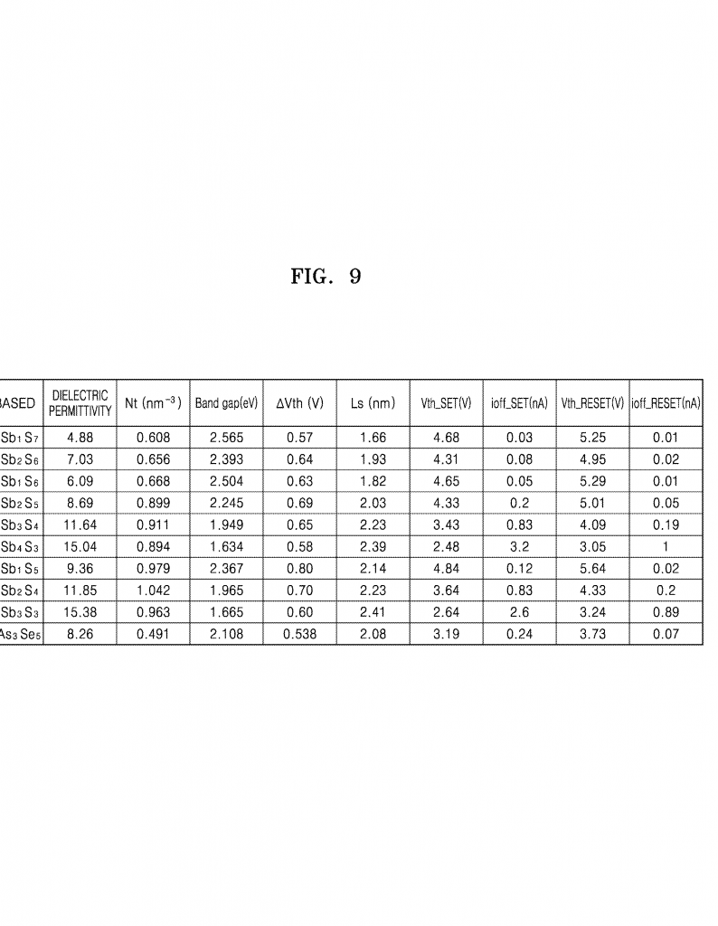
Researchers have also looked for ways to make the memory itself “self-selecting.” That means the memory material can both store data and prevent unwanted currents that could cause errors. This is done by carefully designing the material’s properties, so it only switches “on” at certain voltages and remembers its state until a different voltage is applied. However, many older approaches could not provide a wide enough difference between the “set” and “reset” voltages (called the “memory window”), which limits how reliable the memory can be.
The new invention builds on these earlier ideas but solves several problems at once. It introduces a new SSM material made from Ge, Sb, and S (sulfur), leaving out the toxic or hard-to-use elements. This material is designed to switch at different voltages depending on how much and what direction the voltage is applied. The result is a memory device with a larger memory window, easier manufacturing, and better safety for both workers and the environment.
Invention Description and Key Innovations
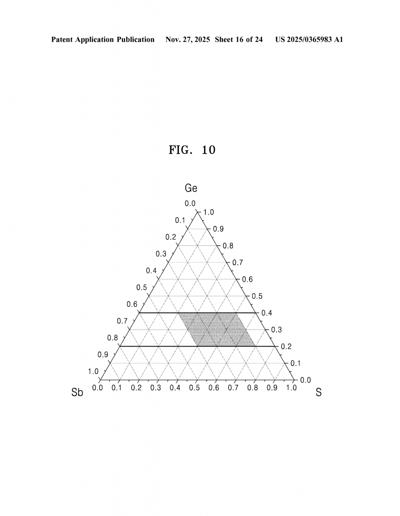
At the heart of this invention is a new SSM material that includes germanium (Ge), antimony (Sb), and sulfur (S). These are all elements that can be safely handled in factories and are already used in the electronics industry. The material is made so that the amount of Ge is between 20% and 40%, and Sb is between 10% and 40%. The rest is mostly sulfur, and sometimes small amounts of other safe elements like nitrogen (N), indium (In), gallium (Ga), aluminum (Al), or silicon (Si) are added, always in small amounts (less than 10%). Importantly, there is no arsenic or selenium in the recipe.
The SSM material shows OTS characteristics. This means it can act like an electrical switch, turning “on” or “off” depending on the voltage applied. But this material is special because its switching voltage (called the threshold voltage) is not fixed. Instead, it can be changed by applying a voltage in one direction or the other, or by changing how strong the voltage is. This lets the memory “remember” data in a new way.
Here’s how it works. When the memory cell is in one state (let’s call it the “low threshold” state), it will turn “on” at a lower voltage. If you apply a voltage in the opposite direction, the cell switches to a “high threshold” state and needs a bigger voltage to turn “on.” The difference between these two threshold voltages is called the memory window. In this invention, the difference is at least 0.5 volts—a big enough gap to make sure the device reliably tells the difference between a “1” and a “0.”
Changing from one state to the other is simple. To switch to the high threshold state (reset), you apply a negative voltage so current flows one way through the cell. To go back to the low threshold state (set), you apply a positive voltage the other way. Reading the stored data is done by applying a voltage that sits between the two thresholds. If current flows, the cell is in one state; if not, it’s in the other.
The magic inside the material comes from “traps,” or tiny places where electrons can get caught or released. The number and type of these traps change when you apply different voltages. For example, applying a positive voltage activates more of these traps near one side of the cell, making it easier for current to flow (low threshold state). A negative voltage deactivates some traps, making it harder for current to get through (high threshold state). This clever trick allows the device to store information without needing a separate selector.
The invention also describes how to build memory devices using this material. You can make a simple two-terminal device: two electrodes (like wires) with the SSM material sandwiched in between. This device can be made into a “cross-point” memory, where many lines cross over each other, and a memory cell is placed at each crossing point. This makes it easy to build very dense memory arrays, which are important for making high-capacity chips.
For even more storage, the invention allows for 3D stacking. Imagine many layers of these cross-point arrays piled on top of each other. The SSM material’s ability to be deposited in thin layers using atomic layer deposition makes this possible. No need for extra selectors means each memory cell takes up less space, so you can fit more data into a smaller area.
What makes this invention truly stand out is its focus on safe, scalable, and efficient memory design. By leaving out arsenic and selenium, it avoids environmental and safety issues. By allowing for atomic layer deposition, it matches the needs of modern chip factories. And by providing a large memory window with reliable switching, it supports the needs of advanced electronics, from smartphones to AI hardware.
The patent also explains that these memory devices can be used in a wide range of products. They fit in regular computers, mobile devices, and even neuromorphic systems—special computers designed to mimic how the brain works. Because the memory is so compact and efficient, it’s especially good for next-generation AI and high-performance computing.
Conclusion
The new self-selecting memory material and device described in this patent are designed for the future. By making memory smaller, faster, more reliable, and easier to manufacture, this invention could help shape the next wave of digital technology. Its use of safe, well-understood elements means it can be made in modern factories without risk to people or the environment. And its clever design allows it to work both as memory and as a selector, streamlining chip architecture for everything from smartphones to AI supercomputers. As the world demands ever more powerful and compact devices, inventions like this one will keep us moving forward.
Click here https://ppubs.uspto.gov/pubwebapp/ and search 20250365983.