SUBSTRATE PROCESSING APPARATUS AND METHOD OF PROCESSING SUBSTRATE USING THE SAME
Invented by YEO; Imbi, PARK; SEYUN, JEONG; SUKHOON
In the fast-changing world of semiconductor manufacturing, even tiny improvements can spark major shifts in technology and business. One such advancement is the substrate processing apparatus described in the recent patent application above. This invention is not just about polishing wafers better; it offers a smarter, cleaner, and more controlled way to handle one of the most important steps in chip making. Let’s break down why this matters and how it works.
Background and Market Context
To understand why this invention is important, we need to look at how semiconductors are made. Every phone, computer, and smart device depends on tiny chips. Making these chips starts with a base called a substrate, usually a thin disk of silicon called a wafer. Before these wafers can be used, they must be very flat and clean. If a wafer is bumpy or dirty, the patterns that make up a chip will not form right. This can ruin the chip and waste money.
One key step is called chemical mechanical polishing, or CMP. In this process, the wafer is placed on a spinning pad, and a special liquid called slurry is poured on top. The slurry contains tiny abrasive particles and chemicals that help smooth and clean the wafer. Polishing makes the wafer flat and ready for building up the layers needed for advanced chips.
As chip designs get smaller and more complex, the need for perfect surfaces gets more serious. Any dust, clump, or leftover material can spell disaster. Factories spend millions to keep wafers clean and flat. At the same time, they need to work fast and not waste materials. This means finding ways to improve every part of the polishing process, including how the slurry is delivered, how the pad is cleaned, and how the equipment stays free from buildup.
Traditional polishing tools face tough problems. The slurry can stick to the parts that spray and spread it, leading to clogs, uneven spraying, or even contamination of the wafer surface. When slurry dries or cakes onto equipment, it can fall onto the wafer and cause defects. Cleaning these tools and keeping them running smoothly is a big cost.
The market is hungry for solutions: tools that can polish wafers more evenly, keep themselves clean, and adjust to different process needs. Equipment that does all this automatically, with fewer breakdowns and less need for operator intervention, is in high demand. This is where the new invention comes in. It addresses real, costly problems that chip makers face every day, promising better performance, less waste, and higher yields.
Scientific Rationale and Prior Art
Now, let’s look at the science behind wafer polishing and what has been tried before. Chemical mechanical polishing uses a mix of physical scrubbing and chemical reactions to smooth the wafer surface. The polishing pad spins, and the wafer is pressed against it. The slurry flows between them, providing both abrasives to grind the surface and chemicals to help reactions that remove unwanted material.
A key challenge is managing the slurry. It must be spread evenly, without waste, and any extra must be removed or recycled. But slurry is sticky and can build up on the nozzles, arms, and other parts that deliver it. This buildup can block the flow, cause uneven coverage, or even drop clumps onto the wafer. Over time, it can harden and become even harder to remove.
To address this, earlier tools have tried different ways to clean or protect the slurry delivery parts. Some used regular water sprays or air jets to wash away buildup. Others used special coatings or materials that resist sticking. Some tools even tried to use steam to help clean and loosen dried slurry. Still, these methods often fell short. Water sprays can only do so much, and steam alone does not always prevent new buildup. Coatings can wear off or react with the chemicals in the slurry.
Another idea has been to use electrostatic forces to control where the slurry goes. By giving surfaces a certain electric charge, it’s possible to attract or repel charged particles in the slurry. Some systems have used this principle to help keep polishing pads clean or to guide the flow of slurry. But these systems have mostly focused on the pad or the wafer, not the delivery arm itself.
In short, past solutions have been limited. They either treat the symptoms of slurry buildup, or they require constant maintenance. None have found a way to combine cleaning, delivery, and charge control in a smart, adjustable system that works in real time. This leaves room for a new approach that brings together steam cleaning, charge control, and precise movement—all key features in the new patent.
Invention Description and Key Innovations
The new substrate processing apparatus is a leap forward because it brings together several clever ideas to solve old problems. Here’s how it works, step by step, and why each part is special.
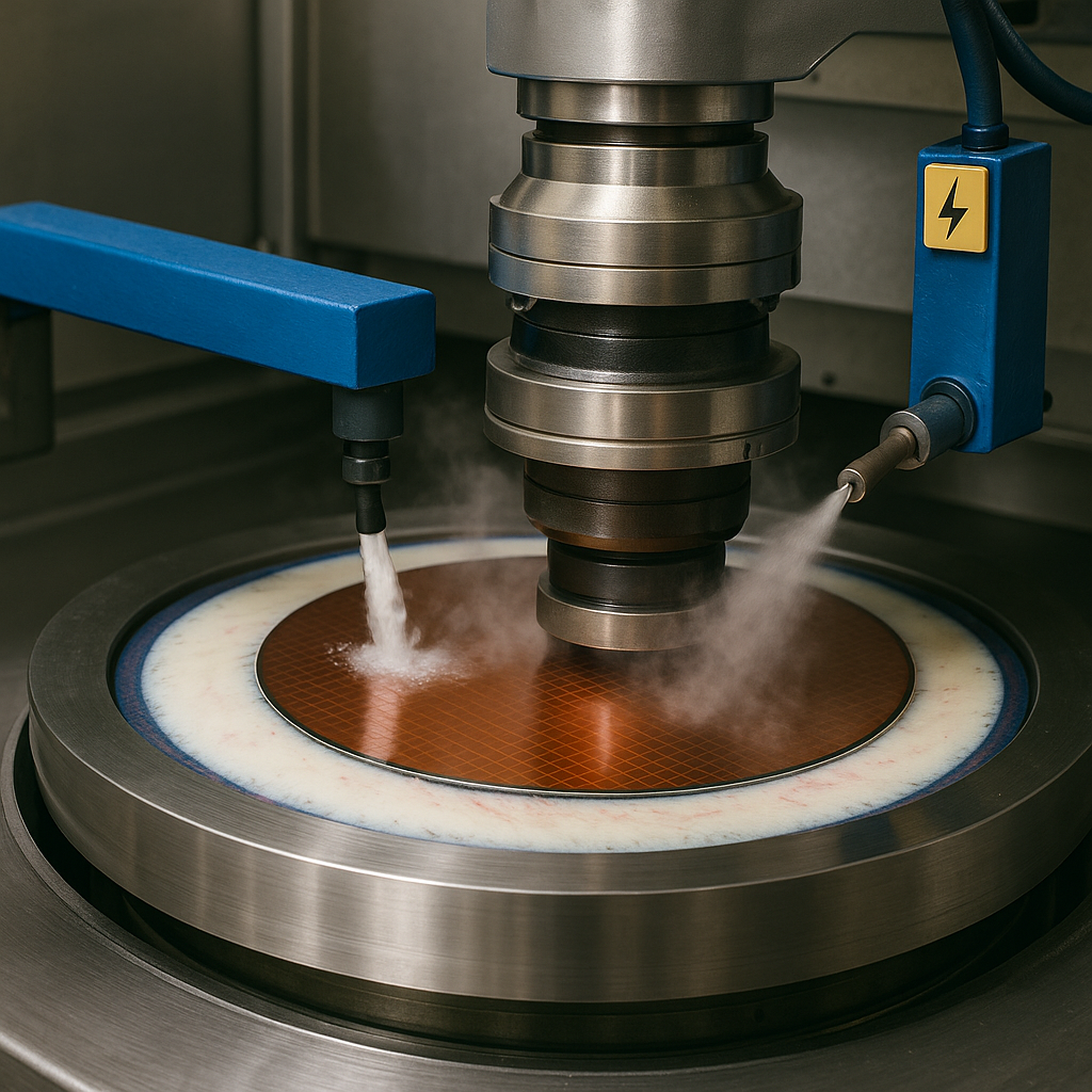
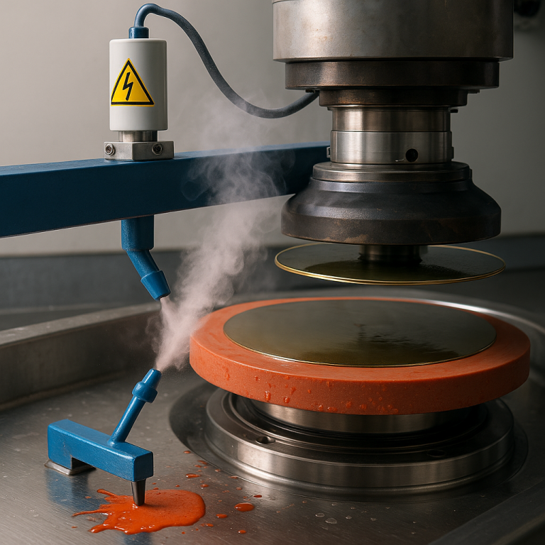
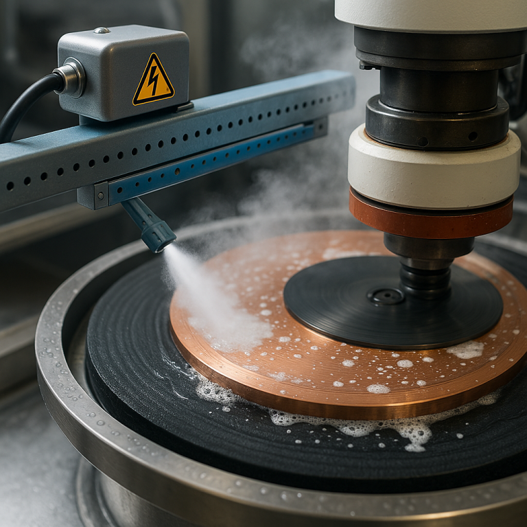
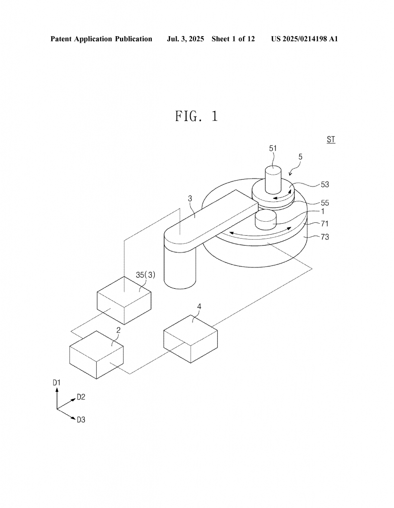
At the heart of the apparatus is the platen. This is a flat, round plate that spins during polishing. On top of it sits the polishing pad, which is where the wafer is placed and polished. Above the pad, a polishing head holds the wafer and can also spin or move as needed.
The real innovation comes with the slurry arm. Unlike older arms, this one isn’t just a tube to pour slurry. It’s a multi-part system designed to keep clean, adapt to different needs, and protect itself from build-up. The slurry arm includes:
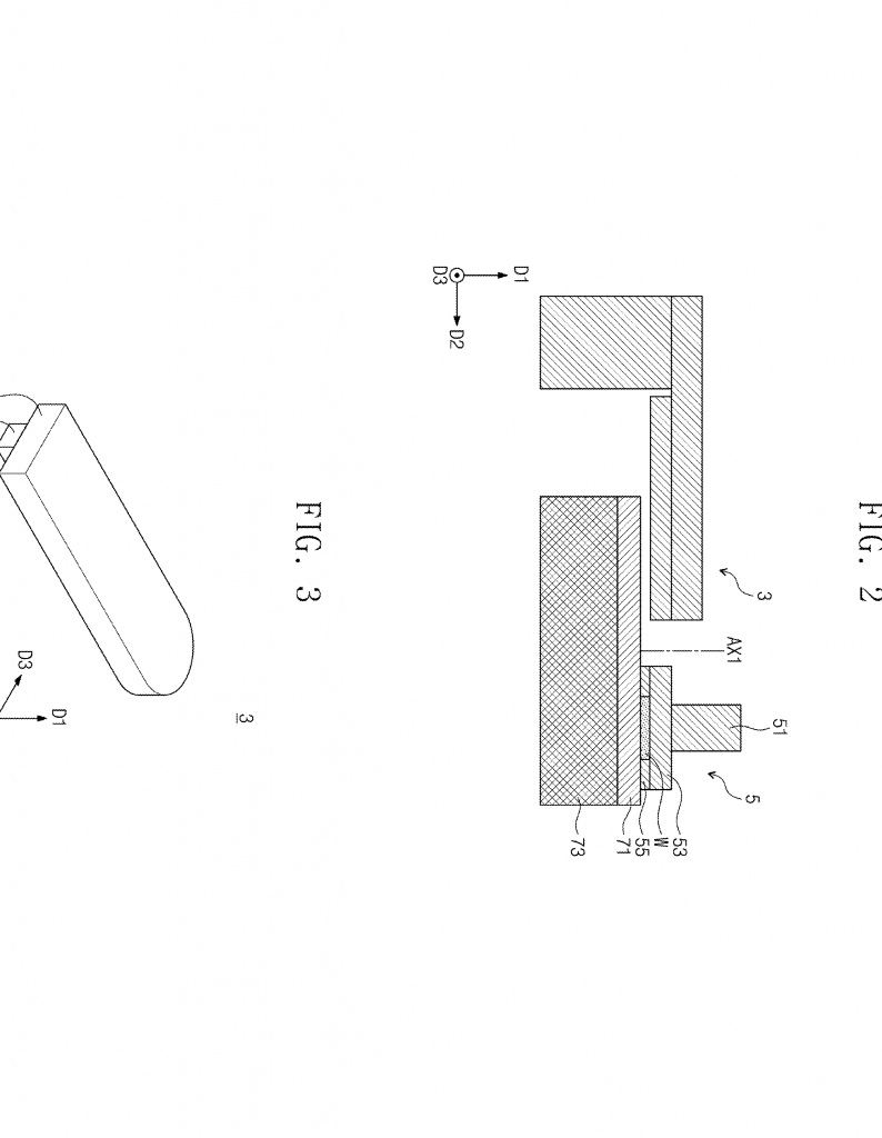
1. Slurry Arm Body: This is the main structure, mounted above the pad. It holds all other parts and can move up, down, or even rotate away from the work area for cleaning or adjustment.
2. Steam Bar: Attached to the arm body, this bar has a special nozzle that sprays steam directly onto the polishing pad or arm area. The steam helps loosen any dried or sticky slurry, making it much less likely to build up. The nozzle can point straight down or be angled to better match the spinning direction of the pad, improving coverage and cleaning.
3. Steam Bar Power Supply: This is what makes the invention really stand out. The steam bar is not just a regular piece of metal—it can be given an electric charge, positive or negative, depending on the type of slurry being used. By matching the charge of the steam bar to the charge of the slurry, the system creates a repelling force. This means the slurry actively avoids sticking to the arm and steam bar, making buildup much less likely. The voltage can be finely tuned, and a controller checks the surface potential in real time to keep everything balanced.
4. Shutter Mechanism: To further control how steam is sprayed, the arm includes a movable shutter. This shutter can change the angle of the steam spray, block it when not needed, or help direct the flow to hard-to-reach spots. It can be adjusted during operation, giving the system even more flexibility.
5. Surface Potential Meter and Central Controller: To keep the system working perfectly, a sensor measures the actual electric charge on the pad or in the slurry. The central controller takes this data and changes the charge on the steam bar as needed. This feedback loop keeps the repelling force just right, no matter how conditions change.
6. Cleaning Sprayer and Arm Driver: When it’s time to clean the arm or steam bar, a special cleaning sprayer can wash it from below. The arm driver lets the whole arm move out of the way for cleaning, or adjust its height to match different types of wafers or processes.
Each of these features brings real benefits. By combining steam cleaning and charge control, the arm avoids sticky buildup, which means less downtime and fewer defects. The smart controls let the system adjust to different slurries and wafers, making it flexible for all kinds of chip manufacturing. The angled steam and adjustable shutter mean that even tricky spots get cleaned. And because the system is automated, it needs less human intervention, making it faster, cheaper, and more reliable.
The patent even includes special filters to protect the steam nozzle, made from materials like polyamide or polyester. This stops abrasive particles from getting into the nozzle and causing damage. Other thoughtful details include the ability to spray cooling gas or water onto the pad, and ways to keep the flow of slurry smooth and even.
Put together, these features turn what used to be a simple delivery arm into a smart, adaptive tool that makes chip manufacturing easier, cleaner, and more efficient.
Conclusion
The substrate processing apparatus described in this patent is a game-changer for anyone making chips or flat substrates. By mixing steam cleaning, electric charge control, and smart feedback, it solves real problems that have long troubled the industry. Factories using this system can expect fewer breakdowns, cleaner wafers, and better yields. It’s an example of how small changes in equipment design can have huge effects on technology and business.
If you work in semiconductor manufacturing, or just want to keep up with the latest in clean tech, this invention is one to watch. It shows that even in a world of tiny electronics, the tools and machines behind the scenes are still ripe for big improvements.
Click here https://ppubs.uspto.gov/pubwebapp/ and search 20250214198.