SUBSTRATE PROCESSING APPARATUS
Invented by YUN; Byoung Min, CHOI; Youn Sok, LEE; Ho Hyun, Samsung Electronics Co., Ltd.

Let’s dive into a new patent for a substrate processing apparatus. This guide will help you understand what it is, why it matters, and what makes it special. We’ll keep things simple and clear, so you don’t need to be an expert to follow along.
Background and Market Context
In factories that make electronic chips and screens, there’s a need for machines that handle very thin slices of material, called substrates. These substrates are used to build things like computer processors and the screens on your phone or TV. The process of making these items involves lots of steps. Workers use big machines to move, clean, and treat these slices. Each step has to be very exact because even a tiny mistake can ruin the whole batch.
Think of these chips and screens like really tiny and detailed puzzles. If one piece isn’t in the right place, the whole puzzle doesn’t work. The same goes for these substrates. They must sit perfectly on a support inside the machine. If they’re off, even by a little, the end product won’t work right. This is why factories use special machines to make sure the substrate is in the right place before they start any process like cleaning, etching, or adding thin layers to it.
Up until now, making sure the substrate is lined up perfectly has been a big challenge. Sometimes, workers use sensors or cameras, but these can be hard to set up or may not work well with different sizes or types of substrates. If the alignment is even a tiny bit off, the whole process can go wrong, wasting time and money. As technology gets more advanced, the need for better, more reliable ways to align substrates has grown. Factories want to make more chips and screens faster and with fewer mistakes. Having a machine that can do this job better helps the factory make more products, with higher quality, and at a lower cost.

This new patent is about a machine that helps solve these problems. It’s designed to make sure the substrate is always in the right spot, every single time. With this, factories can run smoother, make better products, and avoid costly mistakes. As the world uses more electronics, the demand for these kinds of smart machines is only going to grow.
Scientific Rationale and Prior Art
Let’s talk about how these machines have worked before and why the new system is important. In the past, machines used for substrate processing would often use basic sensors or simple cameras. These devices would try to check if the substrate was sitting in the right spot, but they had limits. Sometimes, the sensors would miss small misalignments. Other times, the machines could only handle certain sizes or shapes of substrates. If the factory wanted to change to a different size, it could be a long process to re-adjust everything.
Some older systems used what are called “electrostatic chucks.” These are like special plates that use electricity to hold the substrate in place. While these are good at holding the substrate, they don’t always make sure it’s lined up perfectly. Other machines used vacuum chucks or simple clamps, which have the same problem. The main issue with these older systems is they can’t check and correct the alignment with high accuracy, especially as the sizes of the substrates change or as the processes become more complex.
There have been machines that tried to solve these problems by adding more sensors or using more advanced cameras. Some would use a ring around the edge of the support, called an “edge ring,” to try to help with alignment. But these rings often had a simple design. They didn’t always make it easy for the sensors or cameras to “see” exactly where the edge was, especially if the lighting inside the machine wasn’t good. Sometimes, the sensors would get confused by reflections or shadows.

Another challenge was that earlier machines couldn’t easily adjust themselves. If they noticed a problem, the machine would usually stop and wait for a worker to fix it. This slowed down production and could lead to mistakes if the worker wasn’t careful. Factories want machines that can check, adjust, and fix alignment on their own, without stopping every few minutes.
What makes this new patent stand out is how it addresses all these old problems. It uses a smart alignment sensor with its own imaging units and lighting. The sensor can “see” both the edge of the support and the special edge ring, even if the light isn’t perfect. It can figure out exactly how far apart everything is and adjust itself until it’s just right. Unlike older machines, this system can work with different sizes and can even check multiple points at once, making sure the alignment is good all around the substrate.
This approach is a big step forward. It means less downtime, fewer mistakes, and a more flexible system that can handle the needs of today’s electronics factories. With this, companies can keep up with the fast pace of the tech world, making better chips and screens for all of us.
Invention Description and Key Innovations
Now let’s break down what this new machine does, how it works, and what makes it special. At its core, the invention is a substrate processing apparatus, which is a fancy way of saying it’s a machine that holds and treats thin slices of materials to make chips and screens. But this isn’t just any machine—it has several smart parts that work together to make sure everything is always lined up and ready to go.
Here’s how it works:

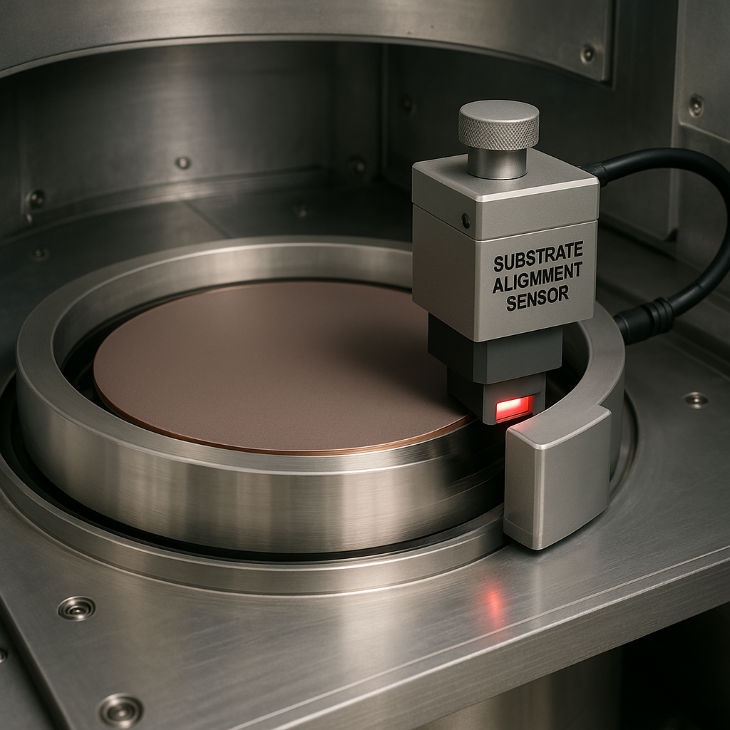
1. Process Chamber and Substrate Support: The machine has a chamber where the substrate goes. At the bottom of this chamber is a support that holds the substrate. Around the edge of this support is a special ring, called the “edge ring.” This ring isn’t just a simple circle. Its top surface has three parts: two flat parts that run side by side, and a third part in between that is slanted. This design helps the sensor “see” the exact edge, making alignment more accurate.
2. Substrate Alignment Sensor: On top of the support, the machine places a special sensor. This sensor is shaped just like the substrate, so it fits perfectly. The sensor has a body, one or more imaging units (like tiny cameras), a control unit (like a small computer), and its own light source. The imaging units are placed in special grooves on the bottom of the sensor, so they can look at both the edge ring and the body of the sensor itself.
3. Imaging and Spacing Calculation: The imaging units take pictures of the edge ring and the side of the sensor body. The control unit uses these images to measure the exact distance between the sensor and the edge ring. It looks for the boundary between the flat and slanted parts of the edge ring, which gives a clear reference point. The control unit then checks if the spacing is the same all the way around. If it’s not, it knows the sensor isn’t centered and makes adjustments until everything is just right.
4. Smart Lighting: The sensor doesn’t rely on the machine’s built-in lights. Instead, it has its own illuminator right in the groove with the cameras. This means the sensor can always get a clear picture, no matter what the lighting is like inside the chamber. The light shines in one direction, and the cameras face another, so there are fewer shadows and reflections to mess up the image.
5. Reference Marks and Multiple Cameras: To make things even more accurate, the sensor has reference marks on its body. The control unit uses these marks to check the measurements in the images, making sure everything is lined up to the tiniest detail. The sensor can have two, three, four, or even more cameras, each looking at a different part of the edge. This way, it can check the alignment all around the substrate, not just in one or two spots.
6. Automatic Adjustment: If the control unit finds that the distances aren’t equal, it moves the sensor until they are. This happens automatically, so there’s no need for a worker to stop the machine and fix things by hand. Once the sensor is perfectly aligned, the machine knows that when it puts the real substrate in, it will also be perfectly aligned.
7. Flexible Design: The system can handle different sizes of substrates and different shapes. The arrangement and number of cameras can be changed depending on what the factory needs. The clever design of the edge ring, with its flat and slanted parts, makes it easy for the cameras to spot the exact edge, even if the substrate or support comes in a new size or shape in the future.
8. Improved Reliability: Because the system checks itself and fixes any problems, factories can trust that every substrate will be in the right place, every time. This means fewer mistakes, less wasted material, and faster production. The machine even keeps track of its own measurements, so if something goes wrong, it’s easy to find and fix the problem.
9. Step-by-Step Process: The way the machine works is simple. First, it puts the alignment sensor in the chamber and lines it up. Once everything is perfect, it takes the sensor out and puts in the real substrate. Since the sensor and the substrate are the same size, the machine knows the substrate will be in the right spot. Then, it starts the real process, whether that’s cleaning, etching, or adding new layers.
10. Smart Control: The control unit inside the sensor isn’t just a simple computer. It’s designed to work with all the parts of the sensor and the machine, making sure everything stays in sync. It can handle different measurement methods, adjust for small errors, and even talk to the rest of the factory’s computer system if needed.
These features make the new machine truly stand out. It’s more accurate, easier to use, and more flexible than anything that came before. Factories can make more products, with higher quality, and spend less time fixing errors or adjusting machines. This is a big win for anyone making chips, screens, or any other products that rely on perfect substrate alignment.
Conclusion
This new substrate processing apparatus is a breakthrough for the electronics industry. By combining smart sensors, precise measurements, and automatic adjustment, it solves the old problems of alignment once and for all. Its flexible design means it can grow with the needs of the factory, handling new sizes and shapes as technology advances. Most importantly, it does all of this in a way that’s simple, reliable, and easy to use. As more and more devices depend on perfect chips and screens, having a machine like this is key to staying ahead in the market. This patent shows the next step in making better, more reliable electronics for everyone.
Click here https://ppubs.uspto.gov/pubwebapp/ and search 20250218842.