SUBSTRATE HOLDING UNIT AND SUBSTRATE PROCESSING APPARATUS
Invented by Byun; Iksu, Kim; Junrae
Today, we’re exploring a new invention for substrate holding units—essential parts used in making semiconductors. These units may sound simple, but they play a huge role in how reliable, clean, and efficient chip-making processes are. Let’s break down what makes this new patent application special and why it matters for the future of electronics.
Background and Market Context
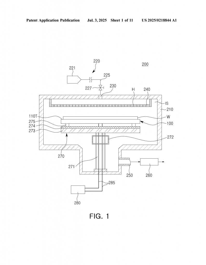
Semiconductors are everywhere. They’re inside your phone, your computer, your car, even your home appliances. The technology behind making these chips is always changing, becoming more complex as chips get smaller and more powerful. At the heart of making these chips are special machines called substrate processing apparatuses. These machines need to hold silicon wafers (which are like thin pancakes) very securely and heat them to high temperatures while keeping everything super clean.
But there’s a problem. When you heat up a wafer on a holder, the holder and the wafer get bigger or smaller as they heat and cool. If they expand or contract at different rates or in different ways, tiny cracks can form where the wafer touches the holder. These cracks can break off tiny pieces—called particles—that ruin the wafer, cause defects, and lower yields. Plus, the surfaces need to be just right: too hard, and the wafer gets scratched; too soft, and the holder wears out fast.
Factories spend a lot of money trying to make sure that their substrate holders (sometimes called chucks or susceptors) don’t cause these problems. They want holders that last a long time, don’t create particles, don’t scratch wafers, and can handle lots of heating and cooling cycles. Improving these holders can save millions every year and help keep the chip-making process running smoothly. That’s why manufacturers are always searching for better materials and designs.
This new patent application addresses these problems head-on. It introduces a substrate holding unit and a related processing apparatus designed to solve the issues of cracking, particle generation, and scratching, all by carefully engineering the materials and structures at the surface where the wafer sits. It’s not just about picking a new material; it’s about how the crystals inside that material are arranged, and how that arrangement can be controlled to match the behavior of the silicon wafer itself. This is a big deal for anyone in the semiconductor business.
Scientific Rationale and Prior Art
To understand why this invention is important, it helps to know how substrate holders have been built up to now, and what their challenges are. Traditionally, substrate holders are made from ceramics like aluminum nitride (AlN) or materials like silicon carbide, alumina, or even graphite. On top of these, thin layers of other materials are sometimes added to help with heat transfer, insulation, or electrostatic clamping (which uses static electricity to hold the wafer in place).
One key measure in picking materials is called the thermal expansion coefficient. This is a number that tells you how much a material grows or shrinks when heated or cooled. The trick is to match the holder’s thermal expansion to the wafer’s, so they both move together as temperature changes. If they don’t, stress builds up, and that’s when cracks and particles happen. But matching this isn’t easy, because not all ceramics are the same, and making very pure, crack-free ceramics is expensive and tricky.
Another issue is surface hardness. If the holder is too hard, the wafer gets scratched. If it’s too soft, the holder wears down fast, creating particles or needing frequent replacement. Some traditional holders use hard coatings, but these can be brittle, and still crack under stress or temperature cycling.
Many of today’s holders use materials like pyrolytic boron nitride (pBN) for insulation, and pyrolytic graphite for heating. Pyrolytic boron nitride is especially popular because it’s clean, stable at high temperatures, and has good electrical properties for holding wafers using static electricity (the Johnsen-Rahbek effect). But even pBN isn’t perfect. Depending on how it’s made, its crystals can line up in different ways—hexagonal or cubic shapes. The hexagonal form is softer and has a negative thermal expansion coefficient (it shrinks when heated), while the cubic form is harder and expands when heated.
In the past, holders have mostly used the hexagonal form because it’s easier to make and less likely to scratch wafers. But this negative expansion doesn’t match silicon wafers, which expand when heated. This mismatch creates stress, cracks, and, eventually, particles.
Some prior inventions tried to fix this by mixing materials or adding coatings, but these solutions often added complexity, cost, or new problems like delamination (layers peeling apart). No one had figured out a way to engineer the surface so it combines both forms—hexagonal and cubic—in just the right amounts and places, to get the best of both worlds: matching expansion, suitable surface hardness, and minimal risk of scratching or particle creation.
Invention Description and Key Innovations
This new patent application changes the game by controlling not just what the holder is made of, but how the crystals inside the material are arranged at the microscopic level. Here’s how it works:
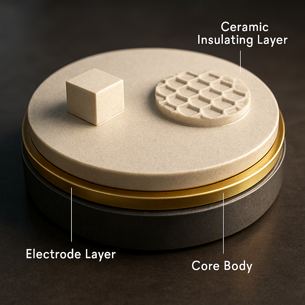
Core Structure: The holder starts with a core body, usually made of graphite or a carbon composite. This gives it strength and helps with heat resistance. On top of this, a first insulating layer is applied, made of pyrolytic boron nitride (pBN). This layer helps insulate the wafer from the core and provides a base for the next layers. Then, a special electrode layer is added—made of pyrolytic graphite—on both the top and bottom surfaces. The top electrode helps grip the wafer electrostatically, while the bottom electrode serves as a heater, precisely controlling the temperature.
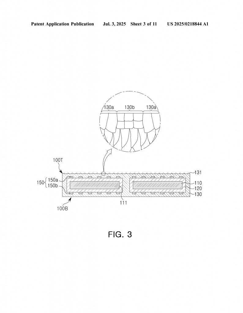
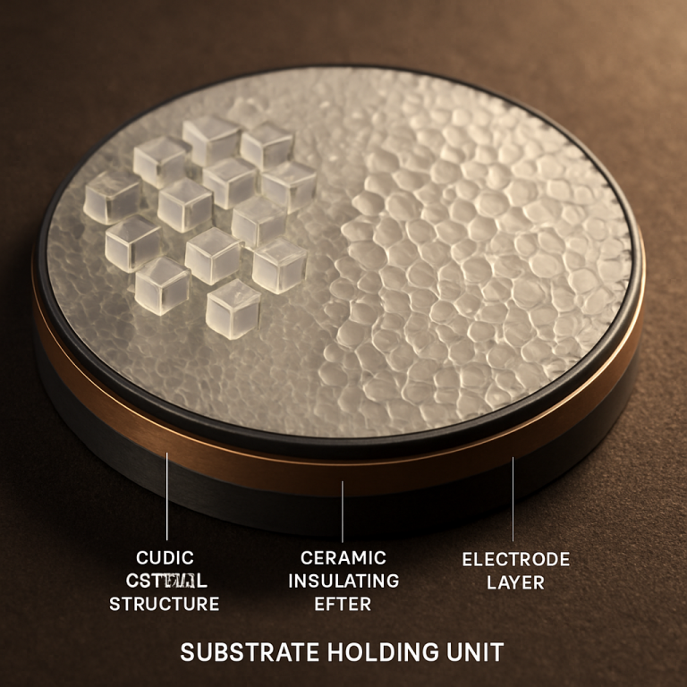
Ceramic Insulating Layer: The real breakthrough is in the outermost ceramic insulating layer, again made of pBN. Here, the inventors use a clever process to control how the pBN crystals grow. After chemical vapor deposition, they heat-treat the layer at very high temperatures and pressures. By adjusting the temperature (between 1700°C and 2400°C) and pressure (1–7.7 GPa), they can tune how much of the pBN forms in the hexagonal shape and how much forms in the cubic shape.
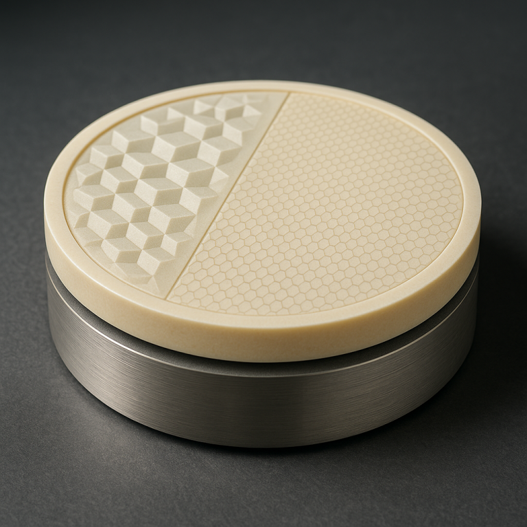
Why does this matter? The hexagonal form is softer and has a negative thermal expansion, while the cubic form is much harder and has a positive expansion (just like silicon). By mixing these two forms in the right ratio (for example, making the cubic form 10–50% of the crystalline region), the surface of the holder now expands at the same rate and in the same direction as the wafer. This simple change means that as the wafer and holder heat up, they move together—no stress, no cracks, and far fewer particles. At the same time, the surface is just hard enough to last a long time, but not so hard that it scratches the wafer. Stiffness (a measure of how hard the surface is) can be tuned to be less than that of silicon, preventing damage.
Advanced Surface Control: The inventors also showed that you can control where the cubic crystals are concentrated. For example, you can have more cubic crystals in the center (where the wafer sits) and fewer on the edges. Or, you can lay them out in patterns, like radial lines. This customization helps further reduce stress and wear, matching the real-world use of the holder.
Protruding Patterns: The surface can be embossed with small, raised patterns. These help with heat and gas flow under the wafer, making the process even more uniform and efficient.
Manufacturing Process: The patent describes in detail how to make these holders. After preparing the core and layering the pBN and graphite, the surface is heat-treated, sometimes with lasers or by annealing, to get the right crystal mix. The process isn’t just theoretical—it’s backed up by data from X-ray and electron microscope studies showing how much of each crystal type is present at different treatment temperatures.
Benefits: The end result is a substrate holder that lasts longer, doesn’t scratch wafers, and produces far fewer particles. The surface expands just like the wafer, so cracks are prevented. Factories can use these holders in a variety of machines, from CVD to etching tools, making them highly versatile.
Key Takeaways for Industry
If you run or supply a semiconductor fab, these innovations mean you can expect:
– Fewer production stoppages due to particle problems or scratched wafers.
– Longer life for your substrate holders, lowering replacement costs.
– Better yields thanks to reduced defects.
– The ability to fine-tune holders for different wafer types or processing needs.
This patent doesn’t just add a new material—it adds a toolkit for engineering the very surface where wafers meet the machine, opening the door to smarter, more reliable chip manufacturing.
Conclusion
Making better chips starts with better tools. This new patent application for a substrate holding unit shows how deep understanding of materials and careful engineering can solve some of the thorniest problems in semiconductor manufacturing. By mixing cubic and hexagonal crystals of pyrolytic boron nitride in just the right way, these holders promise to reduce particles, prevent wafer scratches, and last longer in the toughest environments. For anyone working in or supplying the chip industry, this could be a big step forward—one that’s simple in concept but powerful in its impact.
As the race for smaller, faster, and more reliable chips continues, innovations like this one will be key to keeping production lines running and advancing the state of the art. Watch this space for more developments as the technology moves from patent to factory floor.
Click here https://ppubs.uspto.gov/pubwebapp/ and search 20250218844.