SUBSTRATE HOLDING UNIT AND SUBSTRATE PROCESSING APPARATUS

Invented by BYUN; Iksu, KIM; Yongtae, KANG; Songyun, KIM; Kyungrim, KIM; Junrae, SAMSUNG ELECTRONICS CO., LTD.

In the world of microchips, every detail counts. Tiny changes to the equipment that makes semiconductors can have a big impact on how well chips work and how long they last. This blog explains a new patent application for a special substrate holder—an important device that holds wafers during chip-making. We’ll take a close look at what problem this invention solves, what science and older inventions it builds on, and how it makes things better for chip manufacturing.
Background and Market Context
Semiconductors are at the heart of today’s technology. Phones, computers, cars, and even refrigerators have chips inside them. Making these chips is a very delicate process. It happens inside special machines called substrate processing apparatuses. These machines use heat, special gases, and electricity to build up or etch away layers on thin disks called wafers.
One key part of these machines is the substrate holder, sometimes called a susceptor or chuck. This device holds the wafer steady during processing. The holder often has to do more than just hold—it may need to heat the wafer, keep it in place with static electricity, or protect it from harsh chemicals and plasma. If the holder fails, the wafer could break or get contaminated, which can cost a lot of money.
As chip designs have become smaller and more complex, the demands on substrate holders have grown. They must survive high temperatures, strong electric fields, and exposure to reactive gases. At the same time, even tiny cracks or scratches on the holder can cause serious problems. These defects can damage wafers, create particles, or lead to poor chip yields.
Manufacturers want holders that last longer and require less frequent replacement. Every time a holder is swapped out, production stops. This downtime is expensive. Furthermore, new materials and processes—like plasma-enhanced chemical vapor deposition (PECVD)—put extra stress on substrate holders. Finding ways to make them stronger and more reliable is a top priority for semiconductor companies.
The patent we are discussing addresses these real-world needs. The inventors set out to build a better substrate holder that can handle stress inside the machine, reduce cracks, and extend the holder’s useful life. By doing this, they hope to help chipmakers make more chips, with fewer interruptions, at a lower cost.
Scientific Rationale and Prior Art
To understand why this new substrate holder matters, it helps to know how current holders are made and what their weaknesses are. Traditional substrate holders are built from several layers. Each layer has a job: some provide electrical insulation, some heat the wafer, others create static electricity to hold the wafer in place. The outermost layer is especially important. It faces the wafer and the harsh environment inside the chamber, so it needs to be hard and resistant to heat and plasma.
The problem is that these layers are made from different materials. Each material expands and contracts at its own rate when heated or cooled. If the top layer is very stiff and the layer below is softer or expands differently, stress builds up at the border between the two. Over time, this stress can make cracks form. These cracks can grow and eventually reach the surface where the wafer sits. If that happens, the holder can start shedding particles or even break.
Older inventions tried to deal with this problem in a few ways:
First, some used tough outer coatings, like yttrium oxide or aluminum oxide, to resist wear and plasma. But these coatings are very stiff compared to the layers underneath. The difference in stiffness and how much they expand (called the thermal expansion coefficient) still let stress build up.
Other designs used only a simple insulating layer, often made of pyrolytic boron nitride (pBN), below the coating. pBN is good at handling heat but is softer and less stiff. Again, the mismatch between the soft pBN and the hard outer coating leads to stress at the boundary.
Attempts to make the layers thicker or thinner, or to use different shapes, helped a little, but not enough. The real challenge is that when two materials with very different properties are stuck together and heated up, stress is almost impossible to avoid. If a crack starts at the weak point, it can travel into the hard coating and make the surface unstable.
Some patents have tried to introduce extra layers, like adhesives or flexible films, but these often can’t survive the high temperatures or harsh chemicals used in chip manufacturing. Others have tried to pick materials that are more similar, but this can limit performance in other ways.
What sets this new invention apart is the use of a “buffer layer.” This buffer layer is placed between the stiff outer coating and the softer insulating layer. But it’s not just any layer—it’s made from materials chosen for their “strain energy density.” This means the buffer layer can absorb and spread out the stress that builds up, so cracks are less likely to get through to the surface. The inventors have carefully selected materials and layer thicknesses so that the stress is managed in a new way.
This approach is different from the old methods. Instead of just making things harder or thicker, it manages stress by putting a specially chosen layer in the right place. The science behind it is about balancing the physical properties of all the materials, so the whole stack works together rather than fighting against itself. That’s why this invention represents a meaningful step forward for substrate holders.
Invention Description and Key Innovations
Now, let’s dive into what this new substrate holder actually is, how it’s built, and why it’s better.
The invention is a multilayer substrate holder designed for use in apparatuses that process semiconductor wafers. The holder is made from the following main components:
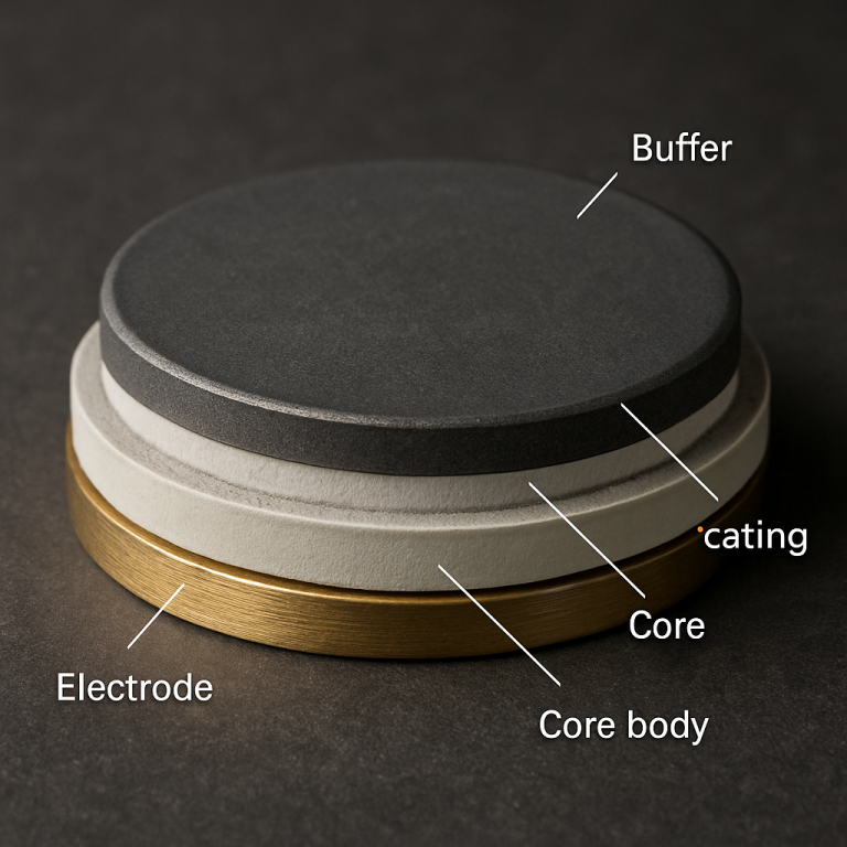
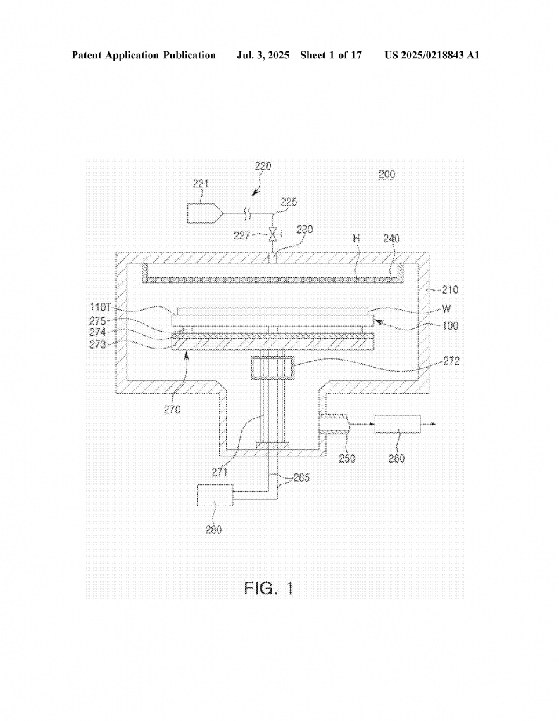
– A “core body” that forms the structure of the holder. This is often made from carbon or a carbon composite like graphite, chosen for its strength and ability to handle heat.
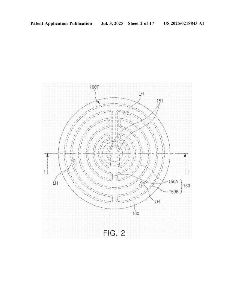
– An “electrode layer” that sits on the top and bottom of the core body. This layer can be used for heating the wafer (acting as a resistor) and for creating the static electricity needed to hold the wafer in place. The electrode layer is typically made from pyrolytic graphite, which conducts well and survives high temperatures.
– A “ceramic insulating layer” covers the electrode layer. The preferred material here is pyrolytic boron nitride (pBN), which is good at insulating, can handle high temperatures, and has a thermal expansion rate similar to the core body. This helps reduce stress between the core and the next layers.
– The “coating layer” is the outermost part. It faces the wafer and the inside of the process chamber. This layer is made from a hard, stiff, and plasma-resistant material—often yttrium oxide (Y2O3), but sometimes other tough oxides, nitrides, or carbides. This layer’s job is to protect the wafer and the rest of the holder from wear and chemical attack.
– The key innovation: a “buffer layer” sits between the ceramic insulating layer (pBN) and the coating layer (yttrium oxide or similar). The buffer layer is made from a material with a lower strain energy density than the coating. This means it soaks up stress and stops cracks from getting through to the top. The buffer layer could be made from things like silicon nitride, yttrium silicate, aluminum nitride, silicon carbide, tungsten carbide, boron carbide, or zirconium carbide.
The inventors didn’t just pick these materials at random. They used simulations and experiments to figure out which materials work best. They found that if the buffer layer’s strain energy density is less than half that of the coating layer, the stress is much lower. Cracks that start in the soft pBN layer are stopped or spread out in the buffer, so they don’t reach the hard coating. This keeps the surface intact, so the wafer is safe.
The thickness of each layer can also be adjusted. Sometimes the buffer is thicker than the coating; sometimes it’s the other way around. In some designs, there are multiple buffer layers, each made from a different material, to control stress even more finely. The buffer layer can even have a multilayer structure, with one buffer material closer to the pBN and another closer to the outer coating, each chosen for its own set of properties.
Another smart feature is that the surface of the coating layer can be patterned with tiny bumps. These bumps help with heat flow and gas movement around the wafer, making the process more efficient.
The patent also describes how to make this holder. It’s a step-by-step process: mold the core, deposit the pBN insulating layers, add and pattern the graphite electrode, deposit more pBN, then add the buffer and coating layers one after the other. Each layer is cleaned and inspected before the next is added, to avoid flaws.
What does all this mean for chipmakers? This new substrate holder should last longer, need fewer replacements, and create fewer particles or defects. That means more chips per batch, less downtime, and lower costs. The holder can also handle higher temperatures and harsher chemistries, which are common in today’s advanced chip processes.
Finally, the new holder design is flexible. It can be used in many kinds of machines: PECVD, standard CVD, plasma etching, and others. The buffer layer strategy can be applied to any process where thermal and mechanical stress are a problem.
Conclusion
This new patent shows how a simple idea—putting the right kind of buffer layer between stiff and soft materials—can solve a long-standing problem in chip manufacturing. By carefully choosing materials and designing the layers to work together, the inventors have made a substrate holder that’s tougher, safer, and longer-lasting. This kind of innovation is critical as the world demands more and better chips for every part of our lives. If you work with semiconductor equipment, or you’re looking for ways to improve yield and uptime, this new substrate holder is worth your attention. It’s a great example of how materials science, engineering, and practical thinking come together to push technology forward.
Click here https://ppubs.uspto.gov/pubwebapp/ and search 20250218843.