SEMICONDUCTOR PACKAGE AND METHOD OF MANUFACTURING SEMICONDUCTOR PACKAGE
Invented by Shin; Seungwan, Lee; Junghyun
Semiconductor packages are the heart of modern electronics. They connect tiny chips to the outside world. A new patent application proposes a fresh way to make these packages stronger and more reliable. In this article, we will break down what this means for the industry and how this idea could change the way your devices work.
Background and Market Context
Today, almost every device you use has a small chip inside. These chips need a home, called a semiconductor package. The package protects the chip and lets it connect to the rest of the device. As technology grows, these chips become smaller, more powerful, and more packed together. This makes the job of the package harder. It must be tough, reliable, and able to fit many connections in a tiny space.
The demand for better semiconductor packages is huge. Phones, computers, cars, and even smart fridges need them. As people want faster and smarter gadgets, the chips inside also get more advanced. This means packages must handle more heat, more connections, and more stress. If a package fails, the whole device can stop working.
One big challenge is making sure the package does not break or lose its connection. Sometimes, cracks or bubbles (called voids) can form inside. This can make the device slow, glitchy, or even dead. Another problem is when layers inside the package start to peel apart (delamination). All these things can ruin a product’s life.
To keep up, companies try new ways to make packages stronger and more reliable. This includes new shapes, new materials, and clever design tricks. The patent we are looking at offers a new way to build the area where the chip connects to the package. This area is important because it handles a lot of stress during use.
In the past, as chips got smaller, the parts that connect them (called pads and bumps) also got smaller and closer together. This made it easier for cracks or voids to appear. The industry has tried to fix this with new films, layers, and building steps. But there is still room for improvement, especially as devices keep shrinking.

If a company can make a package that is more reliable, it can save money, make happier customers, and lead in the market. Devices can be made smaller and lighter, with less risk of failing. This is why new ideas, like the one in this patent, are so important for electronics makers everywhere.
Scientific Rationale and Prior Art
Let’s talk about how semiconductor packages are made and why they sometimes fail. Inside a package, you usually have a chip, some insulating layers, metal pads, and bumps that connect to the outside. The pads are flat pieces of metal that help hold the bumps in place and carry electrical signals.
Traditional pads are simple: they are flat and made from a metal like copper. Sometimes, a thin surface layer is added on top to protect the copper and help the bump stick better. This surface layer might be nickel or gold. Under the pad, there are insulating layers to keep things from shorting out.
Problems start because these different layers can expand and shrink at different speeds when the device heats up or cools down. This can cause stress and lead to cracks, voids, or the layers peeling apart. The place where the pad meets the insulating layer is especially weak. If a crack starts here, it can grow and break the connection.
To fix these issues, engineers have tried several tricks in the past. They have used different surface layers, roughened the surface for better stickiness, and added special films. Sometimes, they change the shape or size of the pad. They have also played with the order in which the layers are built, hoping to reduce stress.
One common method is to add a thin layer of nickel and then gold on top of the copper pad. This helps protect the copper and makes the bump easier to connect. However, even with these tricks, the area where the pad meets the insulating layer can still be a weak point.
Another idea is to use special insulating films that can handle more stress or have better flow to fill gaps. Some companies have tried to make the pad surface rougher so the insulating layer sticks better. These methods help, but they can add cost or complexity.
There have also been attempts to change the pad’s shape. For instance, some designs have made the pad thicker at the edges or rougher at the sides. The idea is to give the insulating layer more area to grab onto. Some have also tried to use special chemicals to etch the pad in different ways.
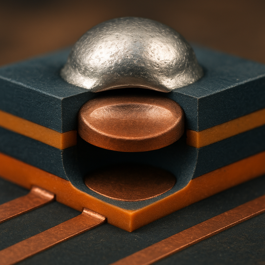
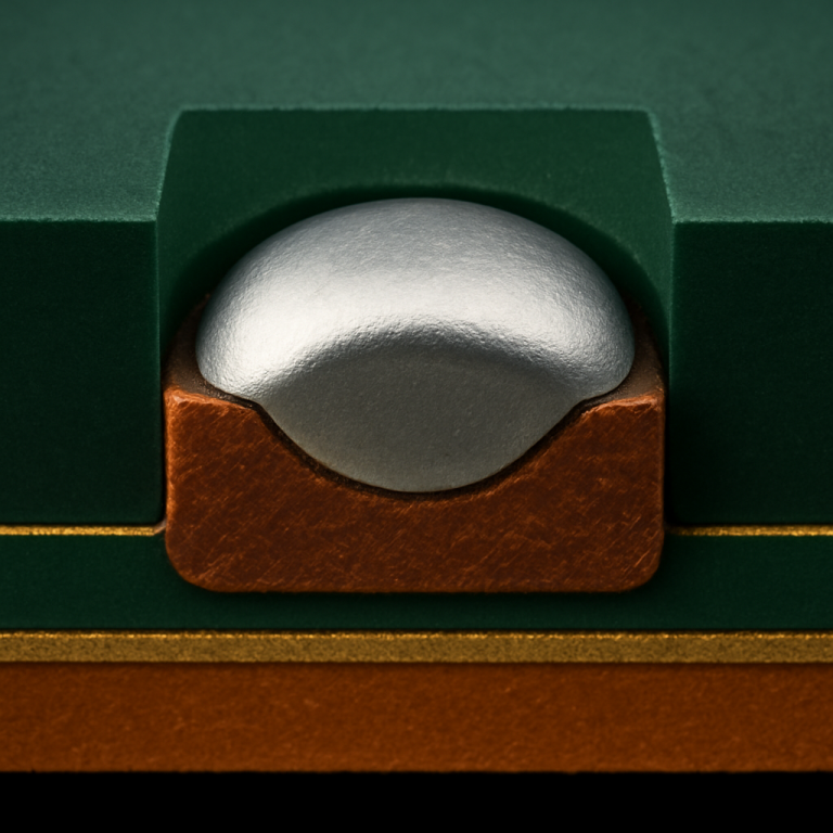
What makes the new patent different is its unique way of shaping the pad and its surface layer. Instead of being flat, the pad’s top is curved inward, like a shallow bowl. The surface layer on top also follows this shape. The center is lower than the edges. This new shape is meant to help the insulating layer stick better and fill any gaps more easily.
The patent also describes a special way to make this shape. It uses a mask to protect the pad’s edges, then uses chemicals to etch away the center, making the curve. After that, the surface layer is added, following the shape. This process is different from the usual flat pad and could be better at stopping cracks or voids from forming.
While there are other patents and papers about making pads more reliable, few have tried a curved shape like this. The focus is on making sure the pad and insulating layer stay together, even when the device gets hot and cold many times. This new approach could be a step forward, especially as devices keep pushing the limits of size and power.
Invention Description and Key Innovations
Now, let’s look closely at what this patent proposes and why it matters. The invention is about a new kind of pad and surface layer for semiconductor packages. Here’s how it works, using simple words.
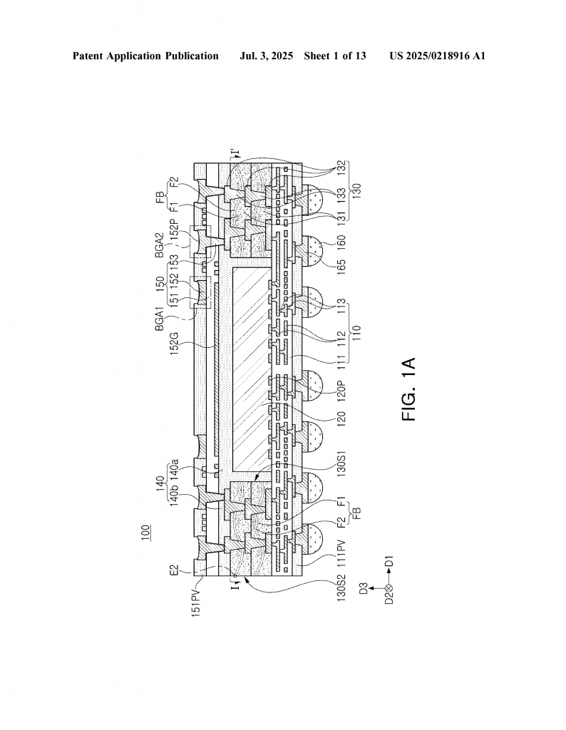
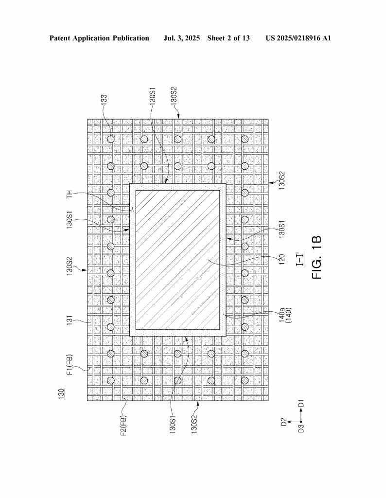
The package starts with two insulating layers. The second layer has a hole or “opening” in it. The pad, which is a small metal piece, sits on top of the first layer and partly covers the opening. On top of the pad, there is a surface layer made from a different metal. This might be nickel or gold, while the pad itself is copper.
The special thing about this design is the shape of the pad’s top surface. Instead of being flat, it is curved inward, like a bowl. This is called “upwardly concave.” The curve at the top is more pronounced than at the bottom, which stays flat. The surface layer on top of the pad follows this curve, so its center is lower than its edges.
This shape is made by covering the pad’s edges with a mask, then using chemicals to etch away the center. After that, the surface layer is added using a plating process, so it matches the shape. The result is a pad with a bowl-like top and a matching surface layer.
Why is this shape important? When the next insulating layer is added, it has an easier time spreading into the bowl shape. This helps fill any gaps between the pad and the insulating layer. It also makes it less likely for cracks, voids, or peeling to start at this spot. The curved shape gives the insulating layer more places to grab onto, which helps keep everything together.
The patent also describes making the pad thinner in the middle than at the edges. This helps make the bowl shape and gives the insulating layer even more area to stick. The side walls of the pad can also be shaped so the upper part is angled more than the lower part. This further helps the insulating layer flow and stick to the pad.
Sometimes, the surface layer on top of the pad is made in two steps. First, a layer of nickel is added, then a layer of gold on top. This helps stop the copper from mixing with the gold and keeps the connection strong. The surface layer might only touch the pad in the center, with the edges not touching. This leaves a small space at the edges, which the insulating layer can fill.
The new design can also include a “seed layer” under the pad. This helps with making the pad in the first place. The seed layer is usually a thin metal like titanium, which is different from the pad and the surface layer.
Once the pad and surface layer are made, the rest of the package is built up. There may be more metal layers for redistribution, more insulating layers, and the chip itself is connected to these layers. The whole package can include bumps for connecting to other chips or to a circuit board.
To sum up, the key innovations are:
– The pad has a curved, bowl-like top surface, not a flat one.
– The surface layer matches this shape, with the center lower than the edges.
– The process uses a mask and chemical etching to make this shape.
– The design helps the insulating layer fill gaps and stick better, reducing the risk of cracks, voids, or peeling.
– Multiple metal layers can be used for the pad and surface, making the connection stronger.
For anyone making semiconductor packages, this idea is actionable. By changing the pad’s shape and using the right metals, you can make a package that stands up better to heat and stress. This means fewer failures, longer device life, and happier customers.
How to Apply This in Manufacturing
If you are making semiconductor packages, you can take a few steps based on this patent. First, consider using a mask and chemical etching to make your pads with a curved, concave surface. Next, use electroless plating to apply your surface layer, making sure it follows the curved shape. Test how well your insulating layer fills the gap and sticks to the pad. Adjust the depth of the curve and the thickness of your metals to get the best results.
You can also experiment with different metals for your surface layer. Nickel and gold are good choices, but other metals might work as well. Make sure your process allows the insulating layer to flow into any spaces between the pad and surface layer. This will help prevent cracks or voids.
Finally, test your packages under heat and stress to see if the new shape really makes a difference. If it does, you can use this design to make your products more reliable and stand out in the market.
Conclusion
The new patent offers a fresh way to make semiconductor packages stronger and more reliable. By shaping the pad with a curved, bowl-like top and matching surface layer, the design helps the insulating layer fill in gaps and stick better. This reduces the risk of cracks, voids, or peeling, which are major causes of device failure. The process uses well-known steps like masking, chemical etching, and plating, so it can fit into existing manufacturing lines. For companies making electronics, adopting this idea can lead to better products that last longer and keep customers happy. As devices get smaller and more powerful, ideas like this will be key to keeping up with the demands of the market.
Click here https://ppubs.uspto.gov/pubwebapp/ and search 20250218916.