SEMICONDUCTOR DEVICES
Invented by LEE; Jung-Han, LEE; Jae-Hwan, KIM; Sang-Su, CHOI; Hwan-Wook, LEE; Tae-Jong, HA; Seung-Mo
The world of semiconductor design is changing fast. Devices are getting smaller, faster, and more powerful. But as chips shrink, new challenges pop up. Today, we’re diving into a recent patent that tackles some of the toughest problems in making fin-type field-effect transistors—also called finFETs. Let’s break down the background, the science, and the unique innovation in a simple and engaging way.
Background and Market Context
To understand why this invention matters, it helps to know how modern chips work. Every phone, computer, or smart gadget you use runs on chips packed with billions of tiny switches called transistors. These switches turn current on and off. As technology has improved, engineers have squeezed more transistors onto each chip, making them smaller and closer together. This has powered the boom in fast, energy-saving electronics.
But making things smaller isn’t easy. As the parts inside a chip get closer, electrical problems start to pop up. If transistors are too close, electricity can leak in ways it shouldn’t. This leakage can cause errors, make the chip run hot, or even break the device. The industry’s answer was to move from flat transistors to 3D shapes. The finFET is one of those answers.
In a finFET, the part that controls the flow of electricity—called the channel—sticks up from the chip like a little fin. This extra height gives engineers more control, so the switches turn on and off more sharply. It’s the standard for the latest chips in phones, computers, and even high-end servers.
But even finFETs have their own set of problems, especially as manufacturers push for even smaller sizes. When you put fins close together, and then try to lay the parts that control them (the gate structures) across those fins, the shapes get tricky. Sometimes, the gate doesn’t cover the fin perfectly. Other times, unwanted connections form between the gate and the parts that bring electricity in and out (called the source and drain). This can cause shorts—basically, the chip stops working right.
The market needs solutions that keep chips reliable even as they shrink. This is not just about making things smaller. It’s about keeping devices running fast, using less power, and staying dependable. Companies that solve these problems gain a big advantage—they can make chips that are more powerful, last longer, and cost less to make.
The patent we’re exploring today is all about solving these headaches in finFETs. It describes a way to build the gate and the “spacer” parts around it so that everything fits perfectly, even at the tiniest sizes. The goal is to stop unwanted shorts and make each transistor work better. Let’s see how the science behind it works, and what makes this solution so special.
Scientific Rationale and Prior Art
For decades, the process of making transistors was based on layering flat materials on top of each other. This worked fine when chips were big. But as the demand for smaller, more powerful devices grew, engineers realized that traditional “planar” transistors couldn’t keep up. They leaked too much current and didn’t turn on and off sharply enough.
The introduction of the finFET structure was a game-changer. In a finFET, the transistor’s channel rises above the surface, like a ridge or fin. This shape gives the gate—the part that controls the current—more surface area to hold onto. It’s like having a hand that grabs from three sides instead of just one. Because of this, finFETs can switch faster and leak less current.
The basic way to build a finFET is to carve out these fins from the silicon base, then lay down a gate structure on top. But as engineers tried to make the fins and the gates smaller and closer together, they found that the shapes didn’t always come out right.
One big problem is with the gate’s lower part. When it gets too close to the isolation layer (which separates the fins), the gate can spread out and form a sort of “skirt” or bulge. This skirt is hard to remove during manufacturing. If left, it can touch the source or drain regions, creating a short—a direct pathway for current that shouldn’t be there. This ruins the transistor.
To stop this, earlier designs used “spacers.” These are extra materials placed around the gate to keep it from touching other parts. But those spacers had their own issues. Sometimes, they didn’t cover the gate’s sidewalls fully, especially at the bottom where the skirt is thickest. Other times, the process to add spacers was too rough, damaging the gate or the fin.
Some patents tried to fix this by building thicker spacers or by adding new etching steps to remove the skirt. But thick spacers take up room, which limits how close the transistors can be placed. Other solutions added complicated steps that made manufacturing more expensive or less reliable.
The crux of the scientific challenge is controlling the shape of the gate and its spacers so that they cover every part of the fin and the isolation layer, but without making the transistor too wide, or the process too complex. The ideal solution would let manufacturers build smaller, faster chips without worrying about shorts or other reliability issues.
This patent builds on all those lessons. It introduces a way to form the gate and its spacers in a step-by-step process. The goal is to make sure that every critical edge and corner is covered, especially where the skirt forms. It does this with a clever arrangement of slopes and widths, and a sequence of etching and layering steps that leave no part exposed. Compared to the prior art, this approach is more precise, uses fewer materials, and fits with existing manufacturing lines.
Now, let’s walk through the heart of the invention and see how it changes the game for finFET design.
Invention Description and Key Innovations
The patent describes a semiconductor device—specifically, a finFET—with a unique way of shaping and covering its gate and the spacers around it. Here’s how it works, step by step, in plain language.
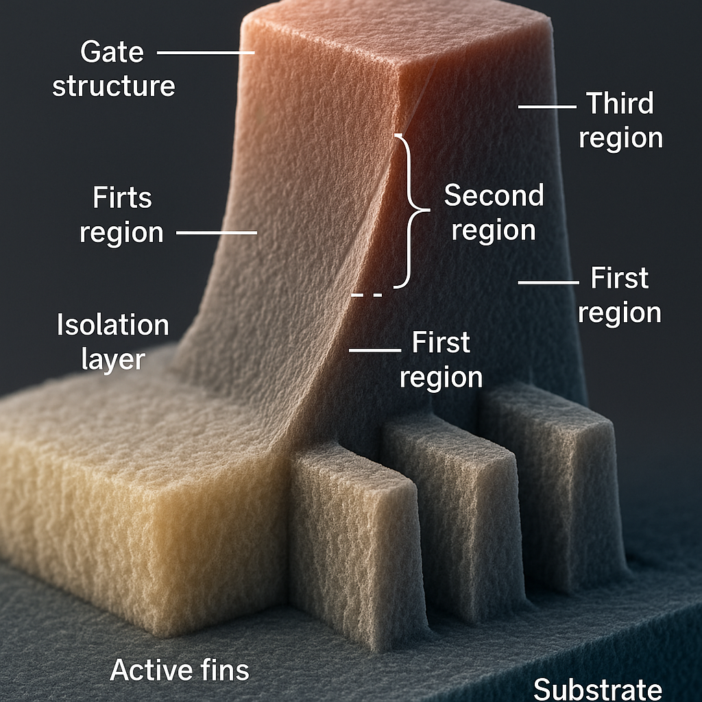
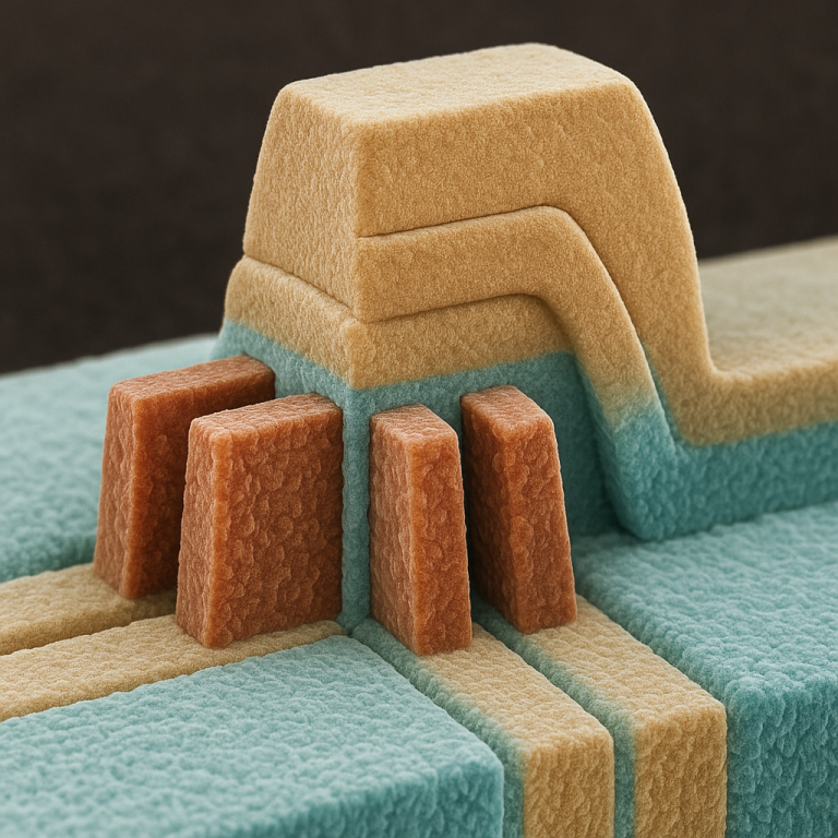
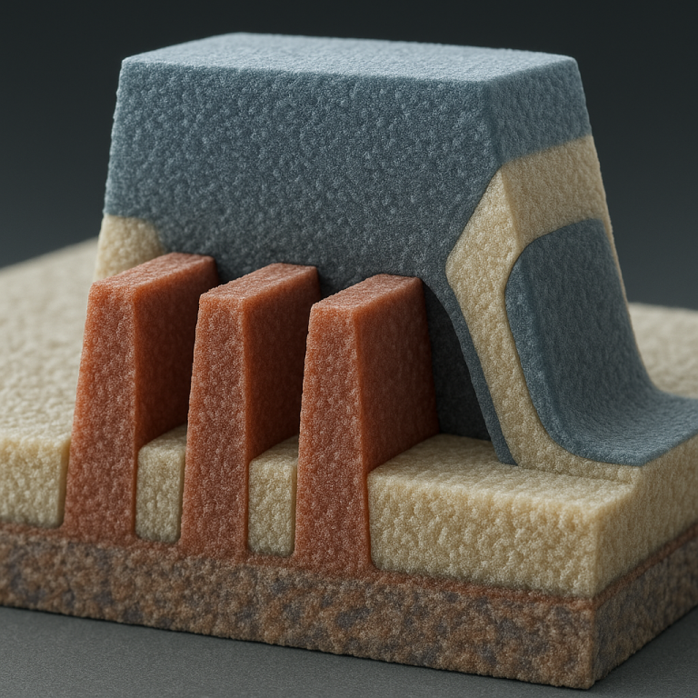
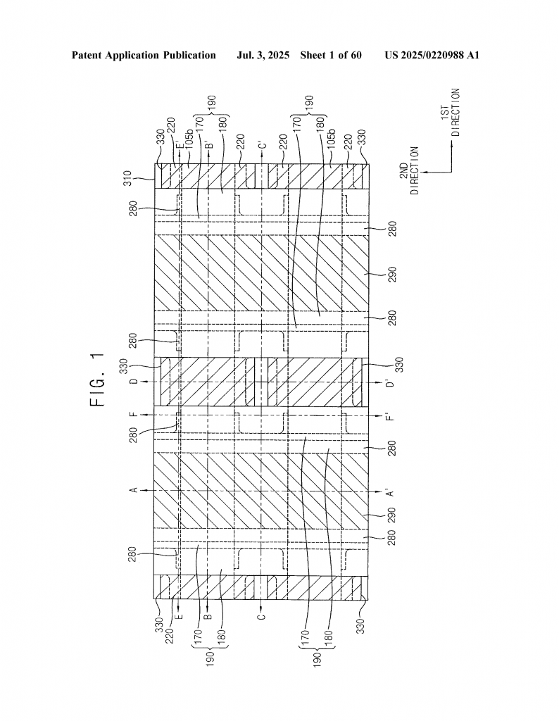
Start with a flat base called a substrate. This can be made of silicon, germanium, or other materials. On top of this, carve out thin, tall strips—the fins—that will serve as the active parts of the transistor. These fins stick up from the surface, separated by an isolation layer. The isolation layer is like the ground between raised garden beds; it keeps the fins from touching each other and leaking current.
Next, lay down the gate structure. This gate crosses over the fins and the isolation layer. The gate is what turns the transistor on or off. In this invention, the gate has two key sections: one that sits over the fin, and one that sits over the isolation layer.
Here’s where the clever part starts. The sidewalls of the gate (the walls that face outward) change shape as they rise up from the isolation layer. Instead of being straight, they are divided into three regions, each with a different slope:
– The lowest part (first region) sticks out the most. Its wall leans outward.
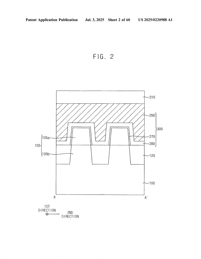
– The middle part (second region) slopes inward as it goes up, getting closer to vertical.
– The top part (third region) is almost straight up and down—about 90 degrees.
This shape means that the gate is widest at the bottom, narrows in the middle, and is narrowest at the top, right where it crosses the fin. This “stepped” design helps in two big ways. First, it makes sure the gate covers the fin perfectly at the top. Second, it leaves enough room at the bottom to fully cover the skirt (that troublesome bulge) with spacers.
To cover these tricky shapes, the invention introduces two types of spacers:
– The first gate spacer hugs the middle and top regions of the gate. It’s thinner and fits neatly into the narrowing space.
– The second gate spacer covers the bottom region and also wraps around the first gate spacer. It’s thicker, filling up the wider area at the bottom.
By splitting up the coverage this way, both thin and thick areas get the right amount of protection—no gaps, no shorts. The spacers can be made from materials like silicon nitride or silicon oxide, which are good insulators and easy to work with in a chip factory.
As the process continues, the gate’s lower exposed parts are etched away using these spacers as masks. This ensures that no part of the gate skirt is left uncovered or in contact with areas it shouldn’t touch. After etching, the thick second spacer fills in any remaining gaps at the bottom. The result: the gate is fully insulated from the source/drain regions, and there’s no path for unwanted current to sneak through.
Another clever aspect is how the process handles the source/drain regions—the areas that bring electricity in and out of the fin. These are made from special materials like silicon-germanium or silicon carbide, which are grown to fill trenches beside the fins. The spacers continue to protect the gate during this step, so the tricky corners where the fin meets the isolation layer stay covered.
Finally, layers of insulation are added above and around the device. Holes are opened where needed, and metal contacts are placed so the transistor can connect to the rest of the chip. Because the gate is perfectly insulated, the chance of a short is almost zero, even as the device shrinks to the tiniest possible size.
The patent also allows for some flexibility. In some versions, the first spacer can be removed after use, leaving only the second, thicker spacer. This can make the process even simpler. The choice of materials for spacers and other layers is open, so manufacturers can adapt the process to their needs.
Overall, the invention stands out for its smart use of slope and width changes, together with a two-spacer design. It solves the key problem of shorts at the base of the gate—an issue that’s plagued finFET makers as devices get smaller. The process is compatible with current factories and doesn’t add unnecessary steps or costs.
In practical terms, chips made with this approach can pack more transistors into the same space, run cooler, and last longer. The improved reliability and smaller size open the door for even faster and more efficient gadgets, from smartphones to servers.
For companies in the business of semiconductor design and manufacturing, adopting this innovation can mean a real advantage over the competition.
Conclusion
The race to build smaller, faster, and more reliable chips continues to push the limits of engineering. This patent presents a smart and practical fix for one of the industry’s most persistent problems: keeping the gate structure and the source/drain regions of a finFET perfectly separated, even as everything shrinks.
By rethinking the shape of the gate and using a two-spacer system, this invention makes it easier to avoid electrical shorts, improve reliability, and support the next wave of chip miniaturization. The approach fits easily into existing manufacturing lines and can be tailored to different needs.
For anyone in chip design, manufacturing, or technology strategy, this is a solution worth watching. It’s a great example of how simple, thoughtful changes in process and structure can deliver big results in the world of advanced electronics.
Click here https://ppubs.uspto.gov/pubwebapp/ and search 20250220988.