PHOTONIC INTEGRATED CIRCUITS WITH SUBSTRATE NOISE COUPLING MITIGATION
Invented by Wang; Zhechao, Vazimali; Milad Gholipour, Liu; Qing
Photonic integrated circuits are getting smarter, smaller, and faster. A new patent now offers a fresh way to make these chips even better by controlling noise and improving connections inside the chip. If you want to know why this matters and how this invention works, keep reading. We’ll break it all down in easy-to-understand language.
Background and Market Context
Today, the world runs on faster and more reliable chips. These tiny pieces of technology are everywhere: in your phone, your computer, the servers that power the internet, and the equipment that helps doctors treat patients. As people use more devices and demand higher speeds, companies are looking for new ways to make chips work better and handle more information without getting bigger or using more power.
One big step forward has been the rise of photonic integrated circuits, or PICs. Unlike regular chips that move signals with electricity, PICs use light. Light is fast, travels far, and does not get mixed up as easily as electrical signals. This makes PICs perfect for high-speed internet, data centers, and even self-driving cars, where huge amounts of information need to move quickly and safely.
But as chips get more complicated, they can start to have new problems. One common issue is called “substrate noise coupling.” In simple words, when you pack many electronic parts close together, the signals from one part can leak into another part through the base layer (called the substrate) that holds everything. This is like having noisy neighbors in an apartment building—the noise can travel through the walls and disturb everyone. For chips, this noise can mess up how parts talk to each other, causing mistakes or slowing things down.
Big tech companies and chip makers are always searching for ways to stop this kind of noise. They want to fit more features into the same chip, but they need to keep the signals clear. That’s why new ideas for controlling noise and improving connections are so important. A chip that can handle more signals without getting “noisy” is worth a lot in today’s market.
This patent tackles that problem head-on. It gives a new way to build PICs so that the electronic parts can be close together but not disturb each other with unwanted signals. It’s like adding soundproof walls between apartments so everyone can enjoy peace and quiet. With this invention, chip makers can build bigger and smarter chips that work better for phones, computers, and much more.
Scientific Rationale and Prior Art
To understand what makes this new invention special, it helps to know how PICs are built and why noise becomes a problem. A typical PIC starts with a strong base, called a substrate, usually made of silicon. On top of this, chip makers add layers of materials that guide light—these are called waveguides and cladding. The waveguides are like tiny roads that carry light from one part of the chip to another. The cladding keeps the light from escaping, much like guardrails on a road.
Inside these chips, you might find lasers, detectors, and other electronic parts. Each part needs to send and receive signals, and sometimes they need to be connected very closely. As more parts are added, the base layer can pick up electrical “noise” from one part and carry it to another. This is not always a problem for simple chips, but as chips get more complex, it can become a big headache.
Over the years, engineers have tried different tricks to solve this. They have used thick layers of insulating material to block the noise, or they have separated the parts as much as possible. Sometimes, they put a simple metal shield between the noisy parts and the rest of the chip. These fixes help, but they come with trade-offs. Thick insulators take up space and make chips bigger. Spreading parts out limits how much you can fit on a chip. Simple metal shields can help, but they are not always easy to connect and may not block all the noise.
Another idea is to use “ground planes”—special layers inside the chip that are always kept at the same electrical voltage. These layers can soak up extra noise. But in many chips, it’s hard to put these planes close enough to where the noise is coming from, or to connect them in a way that makes sense for all the parts in the chip.
Some PICs also use “flip-chip” bonding. This means that a second chip is flipped over and attached directly onto the first chip, with tiny bumps of solder making the connection. This is great for saving space and getting parts very close together, but it can make the noise problem worse, because the parts are now even closer and share the same base layer.
All these earlier ideas have helped, but none of them fully solve the problem of noise traveling through the substrate in complex PICs, especially when you need to connect lots of parts in a small space. Chip makers have needed a better way to combine the best features of all these ideas—insulation, shielding, and good electrical connections—without making chips too big or hard to build.
This is where the new invention comes in. It builds on everything that has come before but adds a new twist, making it easier to keep signals clean while still packing lots of features into one chip.
Invention Description and Key Innovations
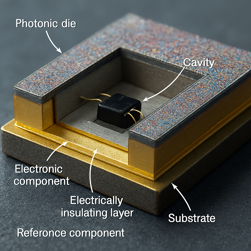
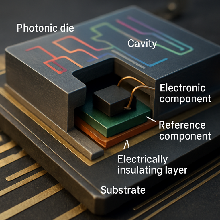
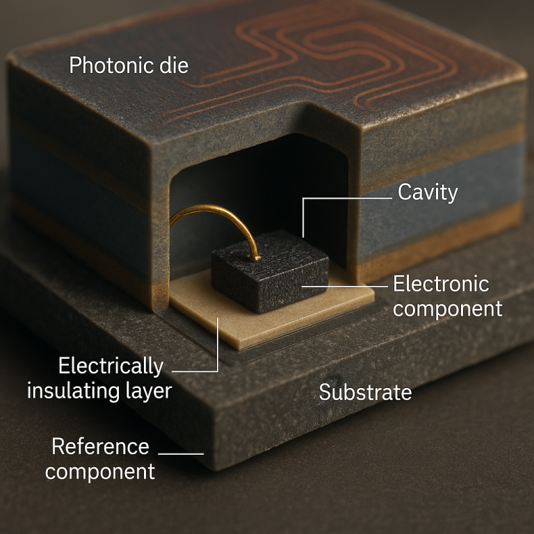
Let’s dig into what makes this invention stand out. Imagine you have a chip—the first photonic die—with its usual base layer, cladding, and waveguide layers. Now, you create a cavity, like a tiny pocket, that goes through these layers down to the base. This cavity is where you can put another electronic part, such as a second photonic die (maybe a laser), or any other electronic part that needs to be close to the main chip.
The magic happens at the bottom of this cavity. The inventor adds a special “reference electrical contact layer.” You can think of this as a shield or a wall that can soak up unwanted noise. This layer is connected to a “reference plane,” which is kept at a steady voltage (like ground). This means it always stays calm, no matter what noisy signals are happening above it.
But there’s more. On top of this shield, the invention adds an electrically insulating layer. This is like a soft mat that keeps the shield from directly touching the next layer. Above the insulator comes the “cavity electrical contact layer.” This upper layer is the one that actually connects to the electronic part you put in the cavity. If you’re using a second chip, like a laser die, it can be attached here—often using tiny blobs of solder called “bumps.”
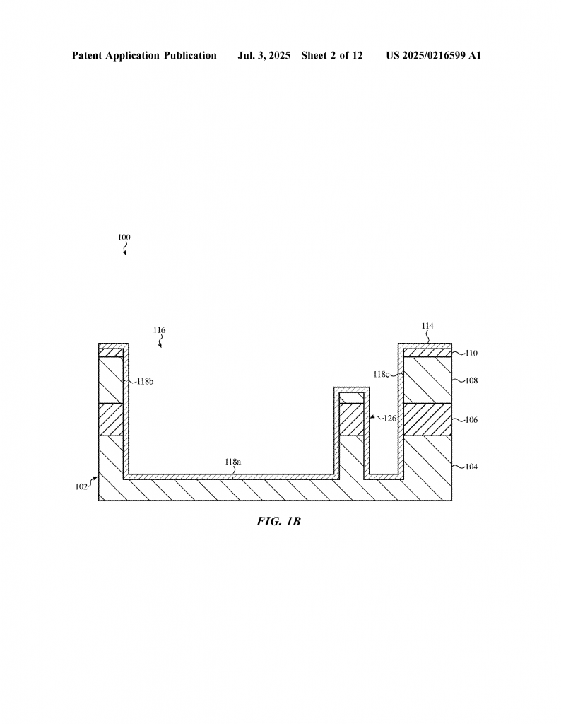
Here’s why this matters: The shield at the bottom of the cavity blocks noise from the base chip, so it can’t reach the sensitive electronics above. At the same time, the insulator means you don’t create any short circuits, and the upper contact can bring in power or signals exactly where they’re needed. It’s a neat sandwich—shield, mat, contact—that lets you connect chips tightly together without letting their signals mess each other up.
The invention also gives you lots of flexibility. For example, the shield layer can be made big enough to stick out beyond the cavity, making it easier to wire up or attach to the rest of the chip. The same goes for the contact layer; if you want to connect it somewhere outside the cavity, you can. If you have more than one part to connect, you can add multiple contact layers and shields, either as separate pieces or as one big shared shield with separate contacts on top.
Sometimes, instead of a separate shield layer, you can even “dope” (add special atoms to change the electrical properties of) the base layer itself, making it work as the shield. This gives you even more options for how to build the chip and connect everything.
Let’s break down some of the main benefits and new ideas in this invention:
1. Better Noise Shielding: By putting a shield layer right under the electronic part, you block noise from below. This makes the chip work more reliably, even as you add more parts.
2. Flexible Connections: The shield and contact layers can be extended outside the cavity, making it easier to connect everything, whether you’re using wires, solder bumps, or other methods.
3. Multiple Parts Supported: You can have several shields and contacts side by side, or use a single big shield for many parts. This is great for chips with lots of lasers, detectors, or other electronics.
4. Fits With Existing Manufacturing: The invention works with common chip-making techniques, like flip-chip bonding and standard materials, so it’s easy for chip companies to use.
5. Customizable for Different Needs: Whether you need a thick shield, a thin one, or a doped region as the shield, you can adjust the design for what works best in your product.
Overall, this invention is like giving every new part in a chip its own private room, complete with soundproof walls and a personal connection to the outside world. It’s a clever way to make chips that are more powerful, more reliable, and ready for the next generation of high-speed technology.
Conclusion
This new approach to building photonic integrated circuits is set to make a big impact. By adding smart noise-blocking shields right where they’re needed, the invention lets chip makers pack more features into every chip without worrying about signal interference. It fits easily into today’s manufacturing lines, making it practical and cost-effective.
If you’re designing or using advanced chips—whether for fast internet, data centers, healthcare equipment, or next-generation consumer devices—this invention could be the key to making your products faster, more reliable, and ready for the future. It’s a simple idea, but one with the power to change how the world’s most important technology is built.
Click here https://ppubs.uspto.gov/pubwebapp/ and search 20250216599.