PHASE MODULATING THIN FILM FOR LONG-WAVE INFRARED THERMAL IMAGING
Invented by HANANIA; Haeri Park, SIDDIQUE; Radwanul Hasan, KUMAR; Shailabh
Thermal cameras help us see heat. But building these cameras has always been tricky and expensive. Now, there’s a new way to make thermal cameras smaller, lighter, and more efficient than ever before. This blog takes you on a journey into the world of metalens arrays with nanostructured thin films, explaining how the technology works and why it matters for the future of thermal imaging.
Background and Market Context
Thermal imaging is a way to “see” heat. It does this by picking up infrared light, which is invisible to our eyes. Thermal cameras are used in many areas — firefighters use them to find people in smoke, doctors use them to spot fevers, and engineers use them to check for overheating parts. Even smartphones now sometimes have small thermal cameras built in.
But making a good thermal camera isn’t easy. The parts that focus heat (called lenses) are usually bulky and heavy. They’re also expensive, often made from special materials like germanium or zinc selenide. These thick lenses are hard to make small. That means most thermal cameras are bigger and cost more than regular cameras.
Today, there’s a growing demand for smaller, lighter, and cheaper thermal cameras. People want to put them in drones, cars, and even wearables. This is where the idea of “metasurfaces” and “metalenses” comes in. Instead of using traditional thick glass or crystal, these new lenses are built from very thin layers of material, only a few millionths of a meter thick. They use tiny patterns — much smaller than the width of a human hair — to guide and focus heat in new ways.
This new approach could change the game. If we can make tiny, cheap, and effective lenses for heat, thermal cameras could become as common as regular cameras. Imagine every phone, car, or robot having a powerful “heat vision” that fits in your pocket or on a chip.
Scientific Rationale and Prior Art
To understand why this new metalens idea is important, let’s take a quick look at how current thermal cameras work and what their limits are.
Normal camera lenses bend visible light using glass or plastic. But infrared light — the kind used for thermal imaging — doesn’t pass through regular glass very well. Instead, special materials like germanium or zinc selenide are used. These materials are expensive and heavy. The lenses themselves often have to be thick to focus the longer infrared waves. That means the final camera is big and heavy too.
Some companies have tried to make “microlens arrays” — small lenses lined up in a grid — to focus light onto each pixel of a sensor. But for thermal cameras, this has been tough. The pixels for heat are usually bigger, and the polymers used for visible light microlenses absorb too much heat, making them useless for thermal imaging.
Scientists have also worked on “diffractive” and “refractive” lenses — types that use very thin layers and special surface patterns to change how light bends. These have worked for regular light, but not so well for the longer waves of infrared heat. The patterns needed are hard to make, and the materials don’t always work at the right wavelengths.
Recently, research into “metamaterials” and “metasurfaces” has opened new doors. These are materials with tiny, human-made patterns that can bend light in ways nature can’t. By carefully choosing the size and shape of these patterns, scientists can control how heat waves move, focus, or scatter.
But even these new metasurfaces had limits: they often required complicated stacks of materials, were hard to mass-produce, or didn’t work across the full range of heat wavelengths needed for real-world thermal cameras.
What’s been missing is a simple, repeatable, and effective way to make thin, lightweight lenses that work perfectly for the most useful part of the heat spectrum — the so-called “long-wave infrared” (LWIR), which covers wavelengths from about 8 to 15 micrometers. This is the sweet spot for most thermal cameras, as it’s where warm objects like people, animals, and machines shine the brightest.
Invention Description and Key Innovations
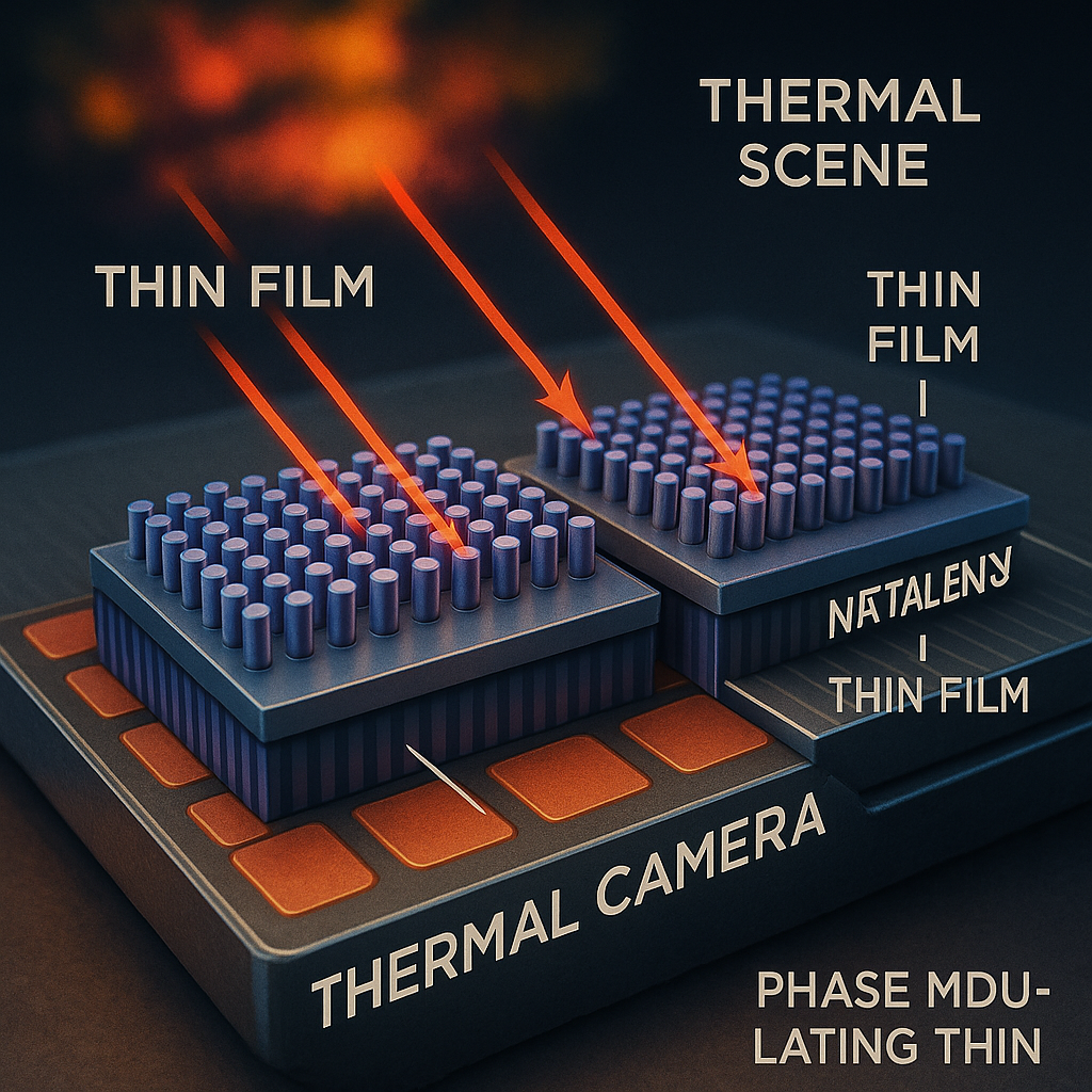
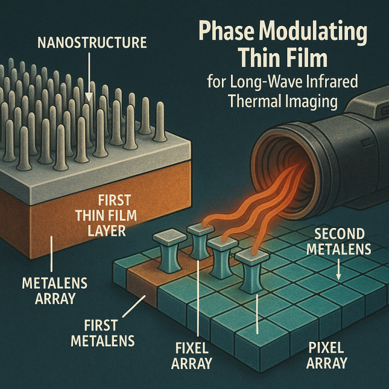
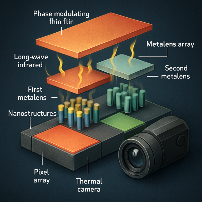
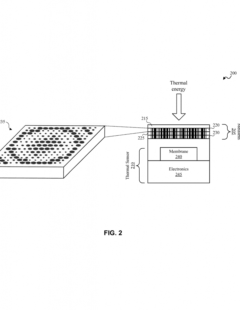
The new invention changes the way we build thermal camera lenses. Instead of using thick, heavy glass or crystal, it uses a thin film — like a very tiny sheet — placed over each sensor pixel. This thin film has a special “nanostructure” built into it.
What is a nanostructure? Imagine patterns so small you can’t see them, even with a regular microscope. These can be tiny holes, pillars (little bumps), or lines (called diffraction gratings). They are arranged in a way that bends, focuses, or directs heat exactly where you want it to go.
Here’s how the invention works:
First, a thin film layer is made from a material that works well for infrared heat, like silicon or a special crystal. Then, using a process like lithography (kind of like making computer chips), the film is patterned with nanostructures. These can be holes that go all the way through, pillars that stick up from the bottom, or special lines on the top or bottom (diffraction gratings).
Each of these tiny features can be as small as a few nanometers (that’s a billionth of a meter) or up to a few micrometers (a millionth of a meter). By carefully choosing the size and spacing of these features, the lens can control heat waves in amazing ways. For example, it can focus the heat tightly onto the sensor, steer it away from unwanted areas, or even block certain wavelengths and let others through.
Several thin film layers can be stacked, each with its own set of nanostructures. Some layers might be made from materials with a high “refractive index” (they bend light more), and others from low-index materials. This stacking allows for even more precise control.
Another clever trick is adding an “antireflective surface” on top. This is a coating made from materials like germanium or zinc selenide, which helps stop heat waves from bouncing away and being lost. It makes sure as much heat as possible goes into the sensor where it can be measured.
Each thin film “metalens” is lined up over a single sensor pixel. This means every pixel in the camera gets its own custom lens, perfectly tuned for its job. The nanostructure for each pixel can even be different, so the camera can correct for odd angles or make sure all the heat is focused just right, no matter where it comes from.
The system is so thin — sometimes just 10 micrometers — that it’s up to 1000 times thinner and much lighter than old-fashioned lenses. Yet, it can shift the phase of the heat wave by up to a full circle (2Pi radians), giving full control over how heat is focused and directed.
This approach brings several big advantages:
First, the camera becomes much smaller and lighter. You could put these in places where regular thermal cameras would never fit — like flying drones, tiny robots, or even in smart glasses.
Second, the system is cheaper to make. It uses processes similar to those already used in electronics, so you can make lots of lenses at once on a single wafer.
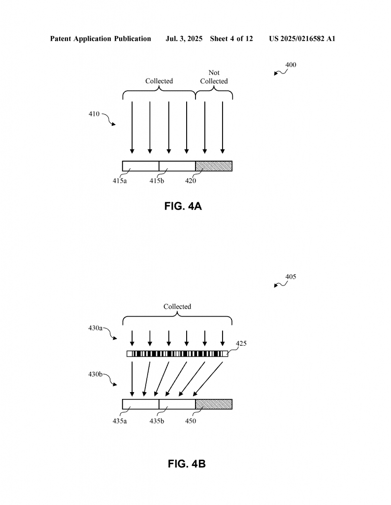
Third, the camera is more efficient. More of the incoming heat actually reaches the sensor where it can be turned into an image. Older cameras wasted a lot of heat, especially at sharp angles. With the metalens array, nearly all the heat is captured and used, making for sharper, clearer pictures.
Fourth, the lens can be tuned for any thermal wavelength, but it works best in the 8 to 15 micrometer range — exactly where most useful heat images are found.
Fifth, the lens can be designed to only let certain wavelengths through, blocking unwanted heat from the sun or other sources. This helps cut down on noise and makes the camera more sensitive.
Sixth, because the nanostructures can be different for each pixel, the camera can correct for tricky viewing angles or odd lighting situations. This means better images, even in tough environments.
Finally, the invention isn’t just for cameras. The same kind of metalens can be used to move heat around in other devices — like spreading heat out from a hot computer chip or focusing it onto a tiny sensor. There are lots of possible uses in electronics, energy, and even medicine.
How is it made?
The process starts with a standard wafer, like the kind used in chip factories. A thin film is formed on top, and a pattern is created using light (lithography). The pattern is etched into the film to make holes, pillars, or gratings. Sometimes, the gaps are filled with another material, and more layers are added. Finally, an antireflective coating is applied. The finished lens is lined up over each pixel of a thermal sensor array and fixed in place.
Because the process is like making chips, it can be scaled up easily and repeated with high precision. That means lots of cameras can be made quickly and cheaply, with every lens exactly where it needs to be.
What makes this new patent special?
There are several key features that set this invention apart:
– Each pixel gets its own customized metalens, not just a single lens for the whole camera.
– The nanostructures can be holes, pillars, or diffraction gratings, or any mix of these.
– The pattern and materials can be varied for each pixel, allowing for full spatial control of the heat waves.
– The thin film can be made from a mix of high and low refractive index materials for even better performance.
– An antireflective layer makes sure as much heat as possible is captured.
– The lens can be tuned for the most useful part of the heat spectrum, the long-wave infrared (8–15 micrometers).
– The whole system is up to 1000 times thinner than traditional thermal lenses, which means lighter cameras and more uses.
Overall, this new metalens array with nanostructured thin films opens the door to smaller, cheaper, and better thermal cameras — and many more devices that need to control heat with precision.
Conclusion
Thermal imaging is becoming more important in our daily lives. But until now, the tools needed were heavy, bulky, and expensive. This new invention changes everything. By building thin, nanostructured metalenses right over each sensor pixel, it’s possible to make thermal cameras that are lighter, smaller, and cheaper — but just as powerful, or even more so, than anything before.
Thanks to clever design and advanced manufacturing, these new metalens arrays can control heat waves in ways never before possible. More heat reaches the sensor, images are sharper, and cameras can fit just about anywhere. The technology is ready to unlock a new era in thermal imaging, putting “heat vision” within reach for everyone, everywhere.
If you’re in the business of cameras, electronics, or even energy management, now is the time to look at metalens technology. The future of thermal imaging is thin, smart, and very, very bright.
Click here https://ppubs.uspto.gov/pubwebapp/ and search 20250216582.