**Next-Gen Pixel Circuit Design Boosts Display Brightness and Efficiency for Consumer Electronics**
Invented by KIM; KWIHYUN, KIM; DONGWOO, LEE; SEHYUN, CHANG; HAKSUN
Introduction
If you have ever wondered how your smartphone, TV, or smartwatch shows such sharp and bright pictures, you’re not alone. The secret is in the display technology, especially in how the tiny parts called pixels light up and show colors. A new patent application from Korea introduces a fresh way to make these pixels work better, use less power, and fit more of them into a small space. This article will guide you through what makes this invention special, why it matters, and how it stands out from older ideas.
Background and Market Context
The world of screens is always changing. Phones, TVs, tablets, and wearables keep getting thinner, lighter, and sharper. This is because people want devices that look great and can do more. At the heart of every screen are pixels—the little dots that make up the pictures you see.
Each pixel has to turn on and off at just the right time, shine at the right brightness, and show accurate colors. For this to happen, every pixel has its own circuit, a kind of tiny engine that controls how it works. These circuits use transistors, which are like switches, to manage power and signals.
Modern screens are expected to show very clear images, even when packed with millions of pixels in a small area. This is called ultra-high resolution. For example, a smartwatch or a phone with a bright, crisp display has to fit a lot of pixels in a tiny space. But as you try to squeeze more pixels onto a screen, you run into problems.
The main problem is that old pixel circuits use many transistors and other tiny parts. The more transistors you use, the more space each pixel needs. When pixels get too big, you can’t fit as many on the screen, and the picture is not as sharp. Also, more transistors mean more power use, which is bad for battery life.
Another challenge is making sure each pixel shines just the right amount. Every transistor is a little different, and over time, their behavior can change. If you don’t fix these differences, some pixels might be brighter or dimmer than others. This makes the picture look uneven.
Companies making displays for devices like smartphones, tablets, TVs, and smartwatches are always looking for ways to solve these problems. They want pixel circuits that are small, use less power, and still make the display look great. The new patent we discuss here is aimed at these issues.
This invention is especially important today as people use screens more than ever. Devices are expected to last longer on a single charge. People want to watch videos, play games, and work on their devices without seeing glitches or faded colors. Also, as wearable devices become more popular, fitting ultra-high resolution screens onto small gadgets is a big deal.
In short, the market wants screens that are sharper, more reliable, and more energy-efficient. Display makers need new ideas to keep up. This invention brings such an idea, promising better screens for all sorts of gadgets.
Scientific Rationale and Prior Art
To understand why this invention is special, let’s first look at how pixel circuits have worked up to now.
In older designs, each pixel has a group of transistors and capacitors. These help decide when the pixel turns on, how long it stays on, and how bright it shines. The most common way to control the brightness is called Pulse Width Modulation (PWM). In simple words, PWM turns the pixel on and off very quickly. The longer it is on during each cycle, the brighter it looks.
But PWM and other methods need extra parts to make sure each pixel works the same way. One big issue is the “threshold voltage” of the transistors. This is the amount of voltage needed to turn them on. If the threshold voltage drifts because of age or slight differences in making each transistor, the pixel can get stuck being too bright or too dim. So, old circuits add extra transistors and capacitors to check and fix this problem. This is called “compensation.”
In some earlier designs, each pixel circuit could have 19 or more transistors and several capacitors, just to make sure each pixel behaves right. This makes each pixel bigger, leaving less space for the actual light emitting part. It also makes the screen use more power and can make the display less sharp.
People have tried to fix these problems in different ways. Some tried to use fewer transistors, but then compensation did not work well. Others kept the number of transistors high, which hurt battery life and made it hard to pack many pixels into a small space.
There have also been attempts to use both P-type (positive) and N-type (negative) transistors. Mixing these types can help lower power use and make the circuit work faster. But getting the right mix, while keeping the pixel small and efficient, has not been easy.
Another area of research has been how to write data to the pixels. Some tried to write both current and voltage to help with compensation. But again, this made the circuit bigger and more complex.
In summary, the main problems with older pixel circuits are:
– Too many transistors and capacitors per pixel.
– Difficulty in fitting lots of pixels for ultra-high resolution.
– High power use, which drains batteries quickly.
– Trouble keeping each pixel’s brightness even over time.
The new patent builds on this background. It takes ideas like PWM and compensation but finds a way to use fewer transistors, mix P-type and N-type in a clever way, and keep the pixels small and efficient. It also uses smart timing to make sure each pixel is set up, written to, and turned on or off at the right moments, all while using less power.
This invention stands on the shoulders of past work but makes important changes that could make future screens much better.
Invention Description and Key Innovations
Now let’s explore what this new pixel circuit does and how it is built differently.
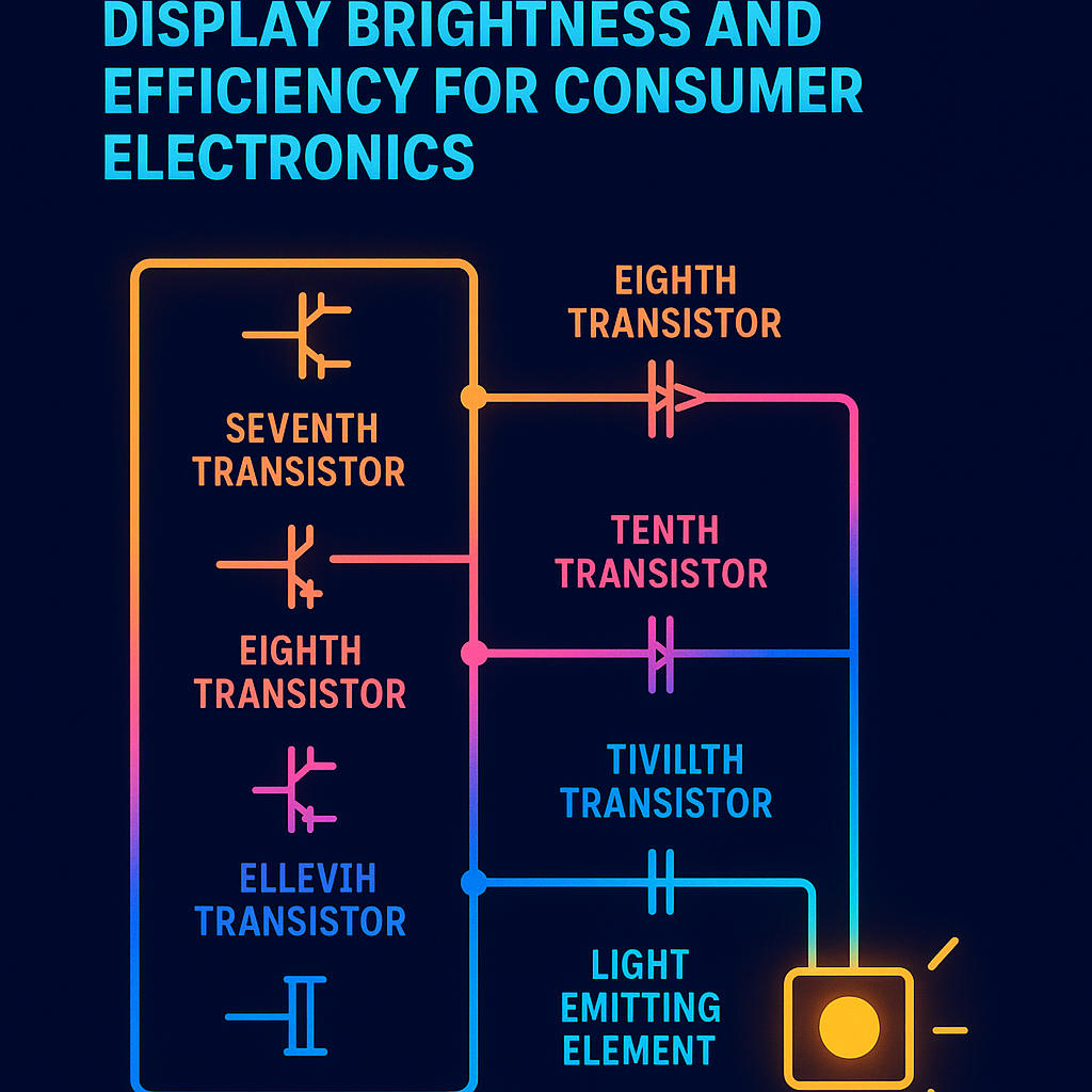
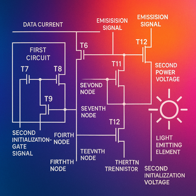
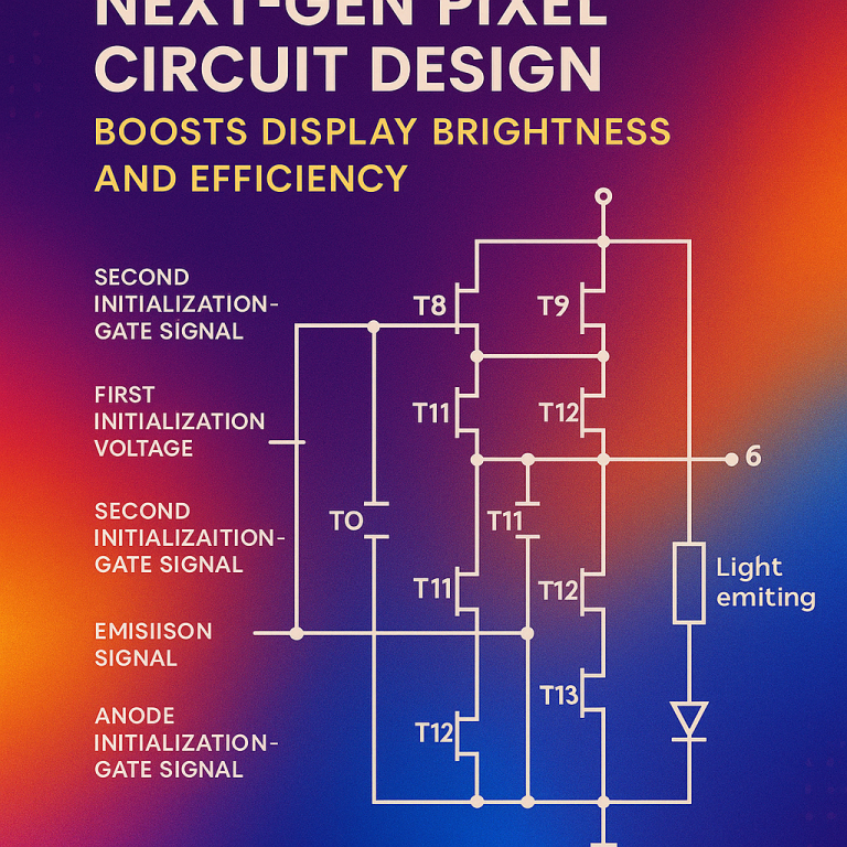
At its core, the invention offers a pixel circuit with fewer transistors and capacitors than older designs. Yet, it still does all the things needed: turning the pixel on and off, setting its brightness, and making sure it stays accurate over time.
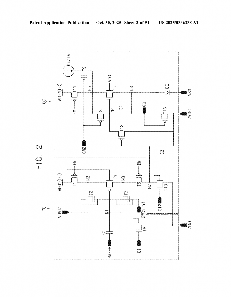
The pixel circuit has two main parts: a constant current generating circuit and a pulse width modulation circuit. These work together to control each pixel.
The constant current generating circuit does the job of making sure the pixel gets the right amount of current, so it shines at the right brightness. The pulse width modulation circuit decides how long the pixel stays on during each cycle, which also controls brightness.
One of the big changes here is the number of transistors. Where old designs could have 19 or more, this new one can use as few as 5 to 13, depending on the version. This makes each pixel much smaller. Smaller pixels mean you can fit more on the screen, making the display sharper. It also leaves more room for the part of the pixel that actually makes light, so the screen can be brighter.
Another change is how the transistors are used. The circuit uses both P-type and N-type transistors in smart places. N-type transistors are good for saving power. By putting them in both the constant current and PWM circuits, the design cuts down on how much energy each pixel uses. This is great for battery life.
The circuit also uses a mix of direct current (DC) and alternating current (AC) voltages to set up each pixel. This helps with the “initialization” step, making sure each pixel starts from the same place every time.
One of the clever parts is how the circuit handles compensation. Instead of needing lots of extra transistors to check and fix the threshold voltage, this design uses the current writing step to do the job. When the pixel is getting set up, the circuit writes a current that matches what the pixel should use. This automatically adjusts for any drift in the transistor’s threshold voltage.
Timing is another area where this invention shines. The pixel goes through different steps:
1. Initialization (setting up the pixel).
2. Writing data and compensation (making sure the pixel will shine at the right brightness).
3. Light emission (actually lighting up the pixel).
4. Light emission-off (turning the pixel off).
By carefully controlling the signals to each transistor at each step, the circuit keeps the pixel working right, even as the screen ages.
The invention also allows for different driving methods. It can work in a normal mode, a variable frequency mode (which helps save power by updating the screen less often when needed), and a progressive scanning mode (which can make moving images smoother).
Another neat trick is that the circuit can be easily changed to use different types of transistors, depending on what is best for the device. For example, in one version, the main “driving” transistor is N-type, and in another, it is P-type. This makes the design flexible for different screen technologies.
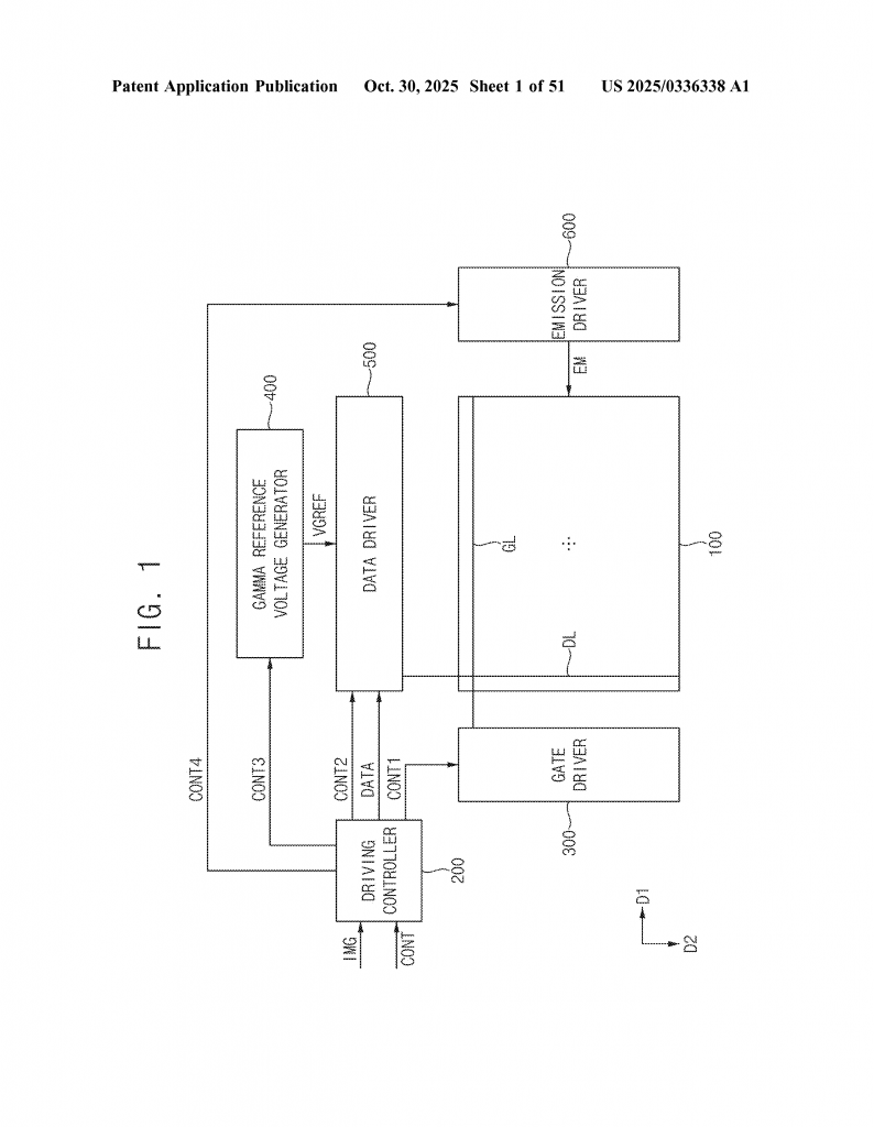
The pixel circuit also works well with the rest of the display system. It connects to a data driver (which sends the picture data), a gate driver (which sends timing signals), and an emission driver (which turns the pixels on and off). All these parts work together to make the screen show the right image at the right time.
Because the circuit is smaller and needs less power, it is perfect for ultra-high resolution screens, like those in smartwatches or the latest smartphones. It also means screens can be brighter, more even, and last longer on a single charge.
In the end, this invention takes a lot of complex engineering and puts it into a simple, small, and powerful package. It solves problems that have held back screen technology and opens the door for better, sharper, and more energy-efficient displays.
Conclusion
This new pixel circuit invention marks a big step forward for display technology. By using fewer transistors, mixing P-type and N-type smartly, and handling compensation in a clever way, it makes pixels smaller, more reliable, and much more efficient. This means sharper screens, longer battery life, and better performance for all sorts of devices—from smartphones to smartwatches and beyond. As the demand for ultra-high resolution displays keeps growing, inventions like this one will shape the future of how we see and use our favorite gadgets. If you care about screen quality or work in the display industry, this is an innovation to watch closely.
Click here https://ppubs.uspto.gov/pubwebapp/ and search 20250336338.