New Memory Tech Boosts Data Speed and Reliability for Next-Gen Electronics Manufacturers

Invented by Garg; Chirag, Filippou; Panagiotis Charilaos, Yang; See-Hun, Apalkov; Dmytro, Jeong; Jaewoo, Ikhtiar; Fnu, Chepulskyy; Roman, Samant; Mahesh

Magnetoresistive random-access memory, or MRAM, is changing the way we store data. But MRAM still faces hurdles—especially as chips shrink and need to work faster and use less power. A new patent application proposes a smart solution: a way to grow special memory cells using “lattice-matched” oxide tunnel barriers and Heusler compounds. In this deep dive, we’ll break down how this invention works, why it matters, and what it means for the future of memory technology.
Background and Market Context
Today, we all rely on memory chips. They run our computers, phones, and even cars. Most of these chips use charge to store data, but this comes with problems. Data can be lost if the power goes out. These chips also wear out, especially as they get smaller. MRAM is a different kind of memory. Instead of charge, it uses magnets. That means it can keep your data safe even if you unplug your device. MRAM is fast, doesn’t wear out like flash memory, and uses less power. It could someday replace both RAM and storage in many devices.
But even MRAM isn’t perfect. The most common MRAM is built using a “magnetic tunnel junction” (MTJ). Picture a sandwich: two thin magnets with a barrier between them. The electrical resistance of this sandwich changes depending on how the magnets line up. This is how you store and read data. But as engineers try to make these sandwiches smaller and more efficient, they run into problems. The materials used for the magnets and the barrier don’t always fit together well on the atomic level. When their “lattice constants”—a kind of atomic spacing—don’t match, it creates strain. This strain can cause defects, which hurt performance and reliability.
The market for MRAM is growing fast. Big companies want memory that is fast, keeps data safe, and uses little power. MRAM promises all of this, but only if scientists can solve the technical problems that come with making the devices smaller and more reliable. The solution in this patent is aimed right at these problems.
Scientific Rationale and Prior Art
To understand this invention, let’s first understand the science behind MRAM and what’s already been tried.
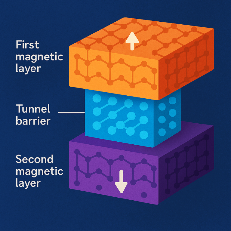
A basic MRAM cell has two magnetic layers and a thin barrier in between. One layer’s magnetization is fixed; the other can be changed (it’s called the “free layer”). When the magnets are parallel, the resistance is low. When they are anti-parallel, the resistance is high. This difference lets you store zeros and ones.
The barrier in the middle is usually magnesium oxide (MgO). MgO has worked well for years because it gives a big difference in resistance between the states, which is called “TMR” (tunnel magnetoresistance). The bigger the TMR, the easier it is to tell a zero from a one.
For the magnetic layers, many devices use cobalt, iron, and boron alloys (like CoFeB). These are ferromagnetic materials. But as engineers push for smaller devices, CoFeB has problems. It doesn’t keep its magnetic direction as well at small sizes and can be hard to switch without using a lot of current.
There’s a better kind of magnetic material: Heusler compounds. Heusler compounds are special alloys that can have high magnetic anisotropy (meaning they keep their magnetic direction well) even in thin layers. Some of them are ferrimagnets, which means their overall magnetization is lower, making them easier to switch. This is very good for power and speed. Heusler compounds also often have “perpendicular magnetic anisotropy” (PMA), meaning their magnetic direction points out of the plane of the chip, which helps in making smaller devices.
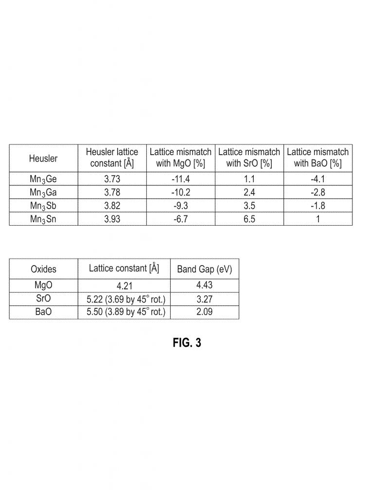
But Heusler compounds and MgO don’t fit together well. Their lattices—the way atoms line up in the crystal—don’t match. This mismatch is often more than 6%. When you try to grow a thin Heusler layer on MgO, the atoms don’t line up. This creates defects, strains, and sometimes even changes the crystal structure of the Heusler. The result? The magnetic properties get worse, the TMR drops, and the device isn’t as reliable.
People have tried to “fix” this mismatch by carefully choosing the seed layer (the first layer you grow) or by changing the growth conditions. But it’s hard to get a perfect match, and the problem gets worse as chips shrink. Some groups have tried other oxides, but not many have focused on picking the barrier so its lattice fits the magnetic layers closely.
Another idea is to use “templating layers”—thin layers that help the next layer grow in the right crystal structure. If you pick a template with the right lattice, you can force the Heusler to grow as you want. But if the barrier is still a poor match, you still get some defects at the barrier interface.
So, while the field has seen lots of progress, no one has nailed down a simple, effective way to get all the layers to fit together with very low mismatch. That’s where this patent comes in.
Invention Description and Key Innovations
This invention introduces a new way to build MRAM cells using Heusler compounds and oxide tunnel barriers that are “lattice-matched.” The main idea is to pick an oxide barrier that fits, at the atomic level, with the Heusler magnetic layers. If the mismatch is kept below 6%, the layers grow together with fewer defects. This gives better magnetic properties, higher TMR, and more reliable memory cells.
Let’s break down how the invention works, using simple terms:
1. The Structure:
Each MRAM cell has a first magnetic layer, a tunnel barrier, and a second magnetic layer. At least one of the magnetic layers is made from a Heusler compound with perpendicular magnetic anisotropy. The barrier is made from at least one oxide, and the key is that the oxide’s lattice matches one or both of the magnetic layers with less than 6% difference.
2. Picking the Right Materials:
The inventors suggest using oxides like strontium oxide (SrO) or barium oxide (BaO) instead of the usual MgO. These oxides have a crystal size much closer to many Heusler compounds. That means when you grow the Heusler on the oxide (or vice versa), the atoms line up better, and you don’t get as many defects.
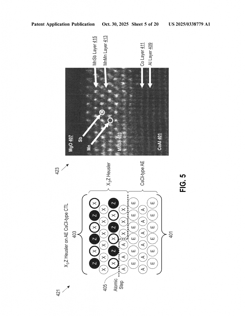
3. Templating Layers:
To make the Heusler compound grow in the right structure, you can use a “templating layer.” This is a thin layer of a material with a crystal structure that matches both the substrate (what you build on) and the Heusler. For example, CoAl can be used as a templating layer for Mn3Ge Heusler. The Heusler layer grown on this template will have the right crystal arrangement, keeping its good magnetic properties.
4. Barrier Engineering:
You can use a single oxide layer as the tunnel barrier (just SrO or BaO), or a double barrier (for example, SrO plus MgO). In the double barrier structure, one oxide matches the Heusler layer, while the other can match a different magnetic material if needed. This gives more flexibility in choosing materials for the top and bottom magnetic layers.
5. Choices for Magnetic Layers:
The invention allows both magnetic layers to be Heusler compounds, or just one, with the other being a more traditional magnetic material like iron or cobalt-iron-boron. This flexibility is important for making devices that suit different needs.
6. The Array:
The invention also covers arrays of these cells, with each cell connected to bit lines and word lines, just like in standard memory chips. The improved cell structure means these arrays can be made smaller, more reliable, and more efficient.
7. Manufacturing:
The patent covers methods for making these cells using standard semiconductor processing steps (like deposition, etching, and patterning). The key step is carefully matching the lattice constants by picking the right oxides and templating layers. This is not a big change from how chips are made today, so it can be adopted by industry quickly.
8. Computer Design:
The invention even covers design files for making these structures using hardware description languages (HDL). This means chip designers can easily add these improved MRAM cells to their designs using computer tools.
What Makes This Invention Unique?
– The focus on lattice matching is new and smart. Instead of just picking materials for their magnetic or electrical properties, the inventors pick them so they fit together at the atomic level. This cuts down on defects and boosts performance.
– The use of SrO and BaO as tunnel barriers is not common in MRAM. By showing that these oxides match Heusler compounds closely, the inventors open up new options for building better memory cells.
– The flexibility to use different combinations of magnetic layers and barriers means the idea can be used in many types of memory chips.
– Covering both the physical structure and the computer design files means the idea is ready for both lab testing and real-world manufacturing.
Benefits:
– Higher TMR: Because the lattice match is good, electrons “tunnel” better, giving a bigger difference between the zero and one states.
– Lower power: The improved structure means less current is needed to switch the memory cell.
– Better scaling: As chips get smaller, the good lattice match keeps the performance high, even at tiny sizes.
– Flexible design: Chip makers can choose from a wider range of magnetic materials and barriers to suit their needs.
Use Cases:
These new MRAM cells could be used in everything from fast cache memory to non-volatile storage in phones and computers, to memory for AI chips and IoT devices. The improved reliability and low power make them a strong fit for future electronics.
Conclusion
The future of memory is all about speed, reliability, and saving power. This patent application makes a big step forward by showing how careful material selection—matching the atomic “lattice constants” of the barrier and magnetic layers—can make MRAM much better. Using oxides like SrO or BaO as the tunnel barrier, along with Heusler compounds and templating layers, solves key problems that have held MRAM back. It makes it easier for chip makers to build smaller, faster, and longer-lasting memory. As the need for better memory keeps growing, inventions like this will help power the next generation of technology.
Click here https://ppubs.uspto.gov/pubwebapp/ and search 20250338779.