New Breakthrough in Detecting Semiconductor Faults Boosts Chip Reliability and Manufacturing Yields

Invented by Endrinal; Lesly Zaren Venturina, Grover; Achin, Kinger; Rakesh Kumar, Google LLC

Let’s talk about a new way to find problems inside the tiny chips that power your phone, computer, and even your car. This patent introduces a design that helps engineers quickly spot and locate tiny cracks or other issues inside these chips, even before they leave the factory. Here’s what you need to know about why this is important, how it builds on past ideas, and what makes this invention stand out.
Background and Market Context
Semiconductor chips are everywhere. They make your phone work, let your computer think, and help your appliances “get smart.” These chips are made by stacking thin layers of special materials, like silicon, on top of each other. Inside, there are millions, even billions, of tiny switches called transistors. The more transistors you can fit, the faster and smarter the chip.
Today, companies try to make chips as small as possible, with as many layers as possible. This is great for making tiny gadgets that do more. But there’s a problem: the tinier these chips get, the easier it is for problems to sneak in. Even the smallest crack or scratch can ruin a whole chip. These faults can show up during the chip-making process, when the chips are cut from big wafers, or even later, when the chips are put into devices like phones or laptops.
Why do these tiny faults matter? A single defect can make a phone freeze, a computer lose data, or a car system fail. The edge of the chip—the very outside part—is especially weak and likely to crack. If a chip with a hidden problem slips past the factory, it could cause devices to break or even become unsafe.
Factories use special machines to look for defects. They use x-rays, ultrasound, and other tools to scan the chips before they get sent out. But as chips get smaller and more complex, these methods can miss very small cracks. Some problems are so tiny they’re nearly invisible, yet they can cause big trouble.
Because of all this, the chip industry is always looking for better ways to check for faults. Catching problems early saves money, makes devices last longer, and keeps customers happy. If a company can find and fix defects before the chips leave the factory, it can avoid costly recalls and protect its reputation.

The market for good, reliable chips is huge and growing. Everything from phones and cars to medical devices and smart home gadgets needs chips that work perfectly. The need to find faults at the tiniest scale, and to do it quickly and cheaply, is more important than ever. This is where the new invention comes in: it gives chip makers a smart way to spot and locate faults, even as chips get smaller and more layered.
Scientific Rationale and Prior Art
To understand what’s new here, it helps to know a bit about how chips are made and how engineers have tried to find faults in the past.
A semiconductor chip is built up layer by layer. Each layer might have different jobs. The bottom layer, called the substrate, is like the foundation of a house. Above this are layers where the chip’s “brains” live—tiny switches, wires, and logic cells that do the actual work. To connect everything, engineers use tiny metal paths called interconnects. These let signals and power flow from one part to another.
In the past, to check for cracks or faults, engineers would often use machines to look at the chip from outside—like an x-ray looking for a broken bone. These tools are good, but they don’t always see very tiny cracks or problems hidden deep inside the chip. Some companies added extra test circuits called “design-for-test” (DFT) structures. These make it easier to check if the chip is working, but they don’t always tell you exactly where a problem is.
The main challenge is that faults can be really small—sometimes just a few atoms wide—and they can happen anywhere: at the edge, in the middle, or between layers. If a crack breaks one of the tiny metal paths, it can stop electricity from getting through. Or, if two paths that are supposed to be separate get connected by accident (a short circuit), the chip can fail.
Previous inventions sometimes put special wires or test points in the chip. These could be checked after manufacturing to see if electricity flowed as expected. But if there was a problem, it was hard to know exactly where it was. Also, as chips became more three-dimensional, with more stacked layers, it got even harder to find faults hiding between layers.
Other methods tried to use advanced imaging—like scanning electron microscopes or acoustic scans—to look for cracks. These methods are slow and expensive, and they still might not find every problem, especially as chips get smaller.
So, the need has been clear: find a way to build into the chip itself a smart structure that not only tells you if something is wrong, but helps you figure out exactly where the problem is, and whether it’s a crack, a break, or a short circuit—right down to the layer where it happened.
That’s where this new patent steps in. It’s not just about checking if a chip works. It’s about knowing which part of the chip is broken, how it broke, and even what kind of defect caused it. This helps chip makers fix their process, improve their quality, and make better products.
Invention Description and Key Innovations
This invention describes a new way to design the inside of a chip so that faults can be found and located very quickly. Here’s how it works, in simple terms.
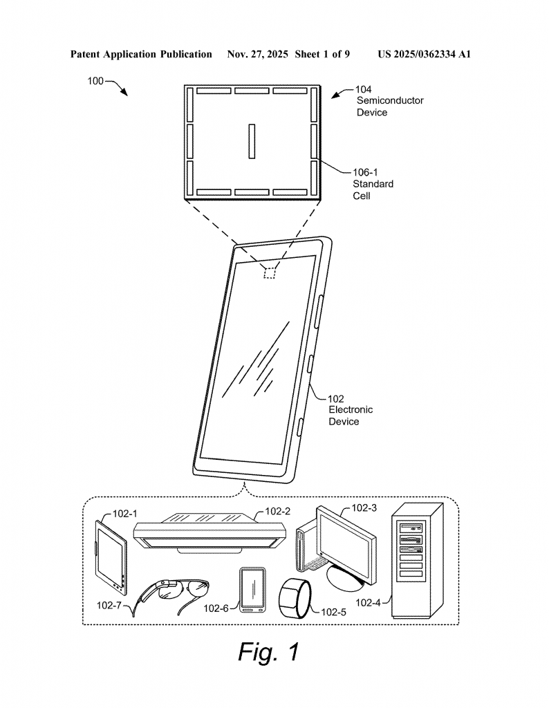
Imagine a chip as a sandwich with many layers. This invention puts special electrical paths—called conductive interconnects—through at least two of these layers. Each interconnect connects to special points on the chip’s surface called terminals. Think of the terminals like the ends of a wire sticking out where you can easily attach a probe or tester.
Inside the chip, these interconnects are set up in a clever way. There can be at least two paths running side by side, sometimes twisting in a pattern like a snake. These paths can be in different layers, and at certain points, they overlap or get very close—even though they are in separate layers. In some versions, they are arranged in a special “serpentine” (twisty) shape, making it more likely that any crack or fault will cross at least one of these paths.
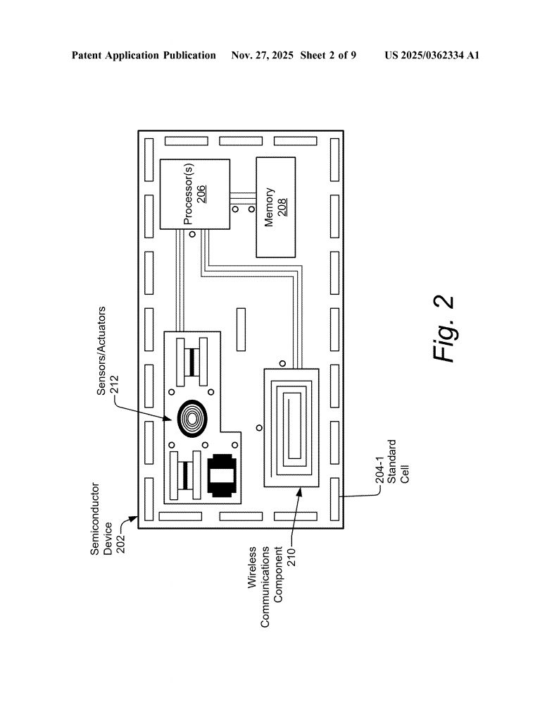
The chip also has special regions called interfacing regions. These can be resistors, tiny channels, or other types of electronic “roadblocks” that let engineers measure things like resistance or voltage very precisely.
When a chip is made, or even after it’s put into a device, a tester can send a tiny current or voltage into one terminal and measure what comes out the other side. If the chip is perfect, the measured value (like resistance or voltage) will be just what you expect. But if there’s a crack, break, or short, the value will be different.
Here’s the clever part: because the interconnects run through different layers and have known shapes, if the tester finds a problem, engineers can often tell exactly which layer is broken and even where the problem is. For example, if two interconnects that should be separate are suddenly connected, it means there’s a short—maybe from a crack or a stray bit of metal bridging the gap. If the measured resistance goes up, it might mean a path is broken somewhere along its length.
The chip can have many of these test structures, placed at locations known to be prone to problems—like along the edge of the chip, or in the middle where the chip might be most stressed. Each structure can be checked separately, helping engineers find not just that there’s a problem, but exactly where it is.
The design allows for a range of different measurements. By checking voltage or resistance between different pairs of terminals, engineers can spot:
- Open circuits (where a path is broken)
- Short circuits (where two paths are connected by accident)
- Changes in resistance that signal a crack, delamination, or other defect
The structures can be used during manufacturing, during testing before the chip is put into a device, or even after the device is in use. This means problems can be caught early, or devices in the field can be checked for faults before they cause a failure.
The patent also allows for the test structures to be hooked up to standard testing systems, like JTAG, which are already used in the chip industry. This means the new design can fit right into existing test procedures, saving time and money.
What makes this invention stand out is how it combines several ideas:
- It uses special interconnects running through two or more layers, so faults in any layer can be found.
- It allows for both open and short faults to be detected, not just one or the other.
- It can pinpoint the location of a fault, not just tell you that something is wrong.
- It works with current chip testing systems, making it easy to use.
By building these test structures right into the chip, the invention helps companies catch problems earlier, fix their manufacturing faster, and make more reliable products. This leads to better phones, computers, and other devices for everyone.
Conclusion
This patent gives the chip industry a smart new tool for finding and fixing problems right at their source. By weaving special test paths through the layers of a chip, it helps engineers catch tiny cracks and faults that older methods might miss. It makes chips more reliable, devices longer-lasting, and gives companies a way to keep quality high even as chips get smaller and more complex. As the world relies more and more on electronics, these kinds of inventions keep us all running smoothly.
Click here https://ppubs.uspto.gov/pubwebapp/ and search 20250362334.