MULTIMODE DOSE COMPENSATION SYSTEM
Invented by PETRY; Klaus, MULLIN; Jacob William, MA; Yan, Applied Materials, Inc.
Ion implantation is a critical process in making the chips that power our phones, computers, and all sorts of electronic devices. But getting it right is tricky. Let’s dive into a recent patent application that tackles some of the biggest headaches in this area, and see how it promises a big step forward for chip makers everywhere.
Background and Market Context
Making computer chips is a lot like building a city, only at a scale so tiny you can’t see it with your eyes. Each chip needs to have certain properties, like how well it conducts electricity. To control this, manufacturers use something called ion implantation. This means firing tiny charged atoms (ions) into the chip material to change its properties. If you get this step wrong, the chip won’t work properly.
As chips have gotten smaller and more complex, the need for precision in this process has skyrocketed. Imagine trying to fill a thimble with a fire hose—that’s how hard it is to get just the right amount of ions in just the right place. Any kind of error, like hitting the wrong spot or using too much force, can ruin the chip.
One of the biggest problems today is non-uniform ion dosing. Sometimes, parts of the chip get too much or too little of the ions, often because tiny changes in the process add up over time. This can happen due to things like gas escaping from the surface (called photoresist outgassing), or because the machine can’t keep the ion beam steady as it moves the chip around. When this happens, manufacturers lose time, waste money, and sometimes have to throw away entire batches of chips.
So, the industry needs new tools and methods that make ion implantation more precise, faster, and less prone to errors. That’s where this new invention comes in. It aims to help chip makers apply ions more evenly and reliably, even as chips keep getting smaller and more complex.
Scientific Rationale and Prior Art
To understand why this invention matters, let’s look at how ion implantation machines work today and where they fall short.
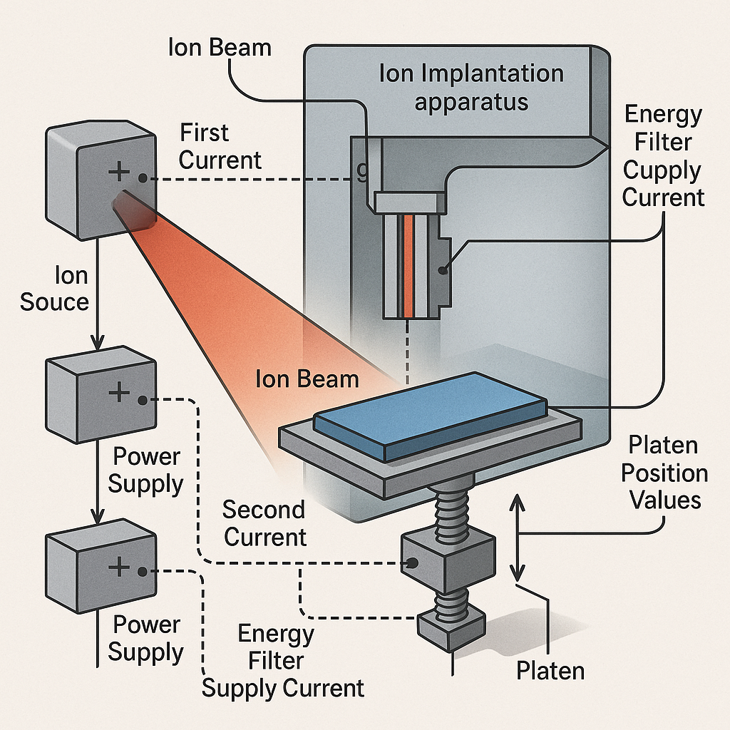
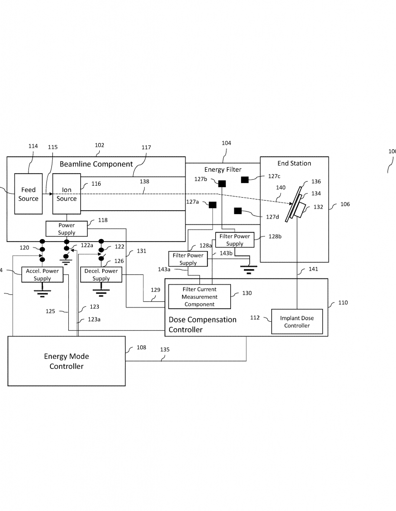
In a typical system, an ion source creates a beam of ions. This beam is then shaped, filtered, and sent down a path (the beamline) to the chip, which sits on a moving platform called a platen. As the ion beam hits the chip, the platform may move around so every part gets treated. Along the way, several components help control the beam:
- Power supplies provide voltages to control how fast the ions move (their energy).
- Energy filters make sure only ions with the right energy reach the chip.
- Controllers try to keep everything in sync, adjusting settings on the fly.
But current systems struggle with a few key challenges:
1. Outgassing and Beam Instability: As the beam hits the chip, gases can escape from the surface. This can mess up the electrical readings that control the beam, making it hard to know if the right dose is being delivered. It’s like trying to fill a glass while the glass keeps moving and changing shape.
2. Slow or Inaccurate Adjustments: Many systems can only adjust the beam or platform in fixed steps, not smoothly. If something goes wrong, they may not notice until it’s too late. This can lead to uneven ion doses.
3. Limited Feedback Loops: Often, these machines don’t have a fast, smart way to measure what’s happening in real time and adjust their actions. They’re like cars without good speedometers or steering wheels—they can go fast, but not always where you want.
Other inventions in the past have tried to fix some of these problems. For example, some systems use extra sensors or computers to watch the beam and the platform, trying to keep things steady. Others focus on filtering out bad readings or making the platform move more smoothly. But these solutions often add cost and complexity, or don’t work well when making very advanced chips.
What has been missing is a truly integrated approach: a system that watches all the key currents and voltages in the machine, figures out exactly how the beam is behaving, and then moves the platform or tweaks the filters in real time to keep everything just right. That’s where this patent application comes in.
Invention Description and Key Innovations
This new invention introduces a smarter, more responsive way to control ion implantation. Let’s break it down into simple parts.
1. Smarter Power Control
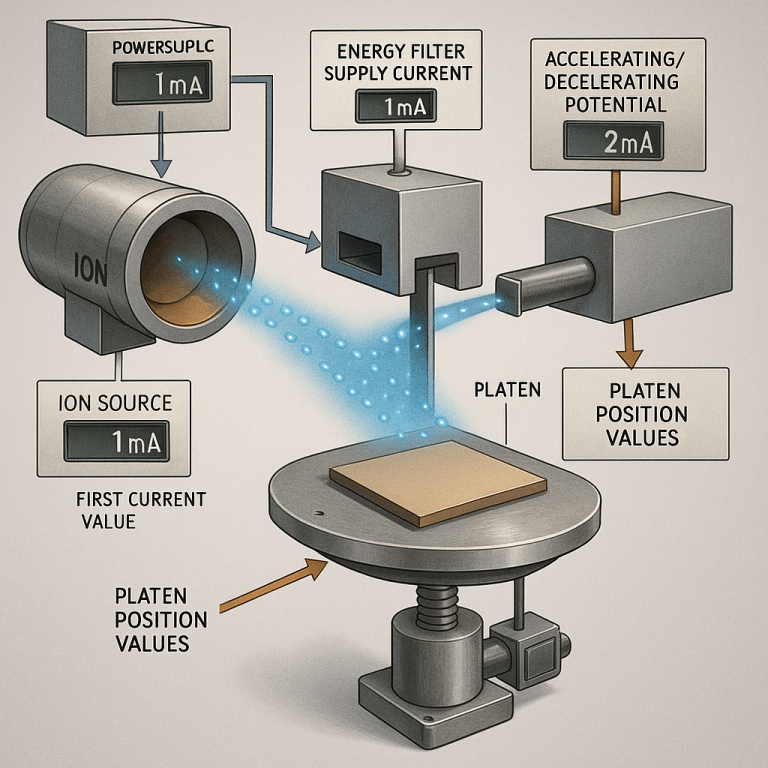
The system uses several power supplies:
- One powers the ion source, setting up the basic beam.
- Others can either speed up (accelerate) or slow down (decelerate) the ions after they’re created. Only one of these is active at a time, making the system simpler and less prone to error.
2. Real-Time Energy Filtering
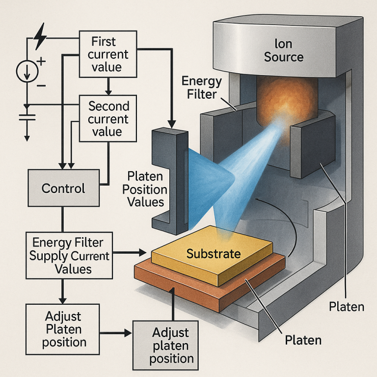
Between the ion source and the chip, there’s a special energy filter made up of electrodes. These electrodes can change the beam’s direction, focus, and energy. The system watches the electrical currents going to these electrodes very closely. By doing so, it knows exactly how the beam is behaving at every moment.
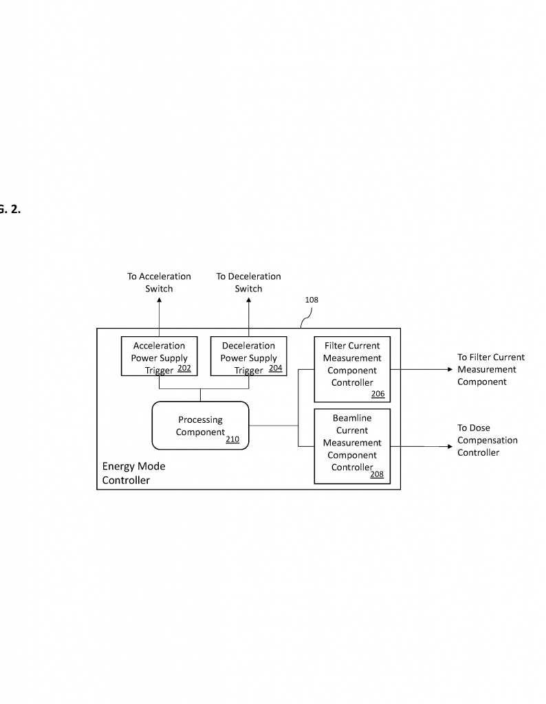
3. Dose Compensation Controller
The heart of the invention is a controller that acts like a smart traffic cop. It continuously gathers:
- The current powering the ion source.
- The current from the accelerating or decelerating supply.
- The current going to the energy filter electrodes.
By looking at these numbers, the controller can figure out if the beam is too strong, too weak, or hitting the chip in the wrong place. It then calculates how to move the platen—or adjust the filter settings—so the right dose always goes exactly where it should.
4. Dynamic Platen Adjustment
Instead of moving the chip in fixed steps, this system can adjust the platen’s position in real time, based on live feedback. If the system detects that part of the chip is getting too much or too little dose, it can speed up, slow down, or reposition the platform instantly. This means much more even treatment, fewer errors, and less waste.
5. Integrated Feedback for Uniformity
The system doesn’t just react to problems—it anticipates them. By constantly comparing the sum of all the key currents to what it expects, it can spot issues before they cause bad chips. If outgassing or other effects start to skew the readings, the controller can compensate by adjusting either the platform or the filter settings, keeping everything on target.
6. Software and Hardware Synergy
All of this is managed by a set of processors and storage units running special software. The software can be updated, customized, or even distributed across several computers, meaning the system can be upgraded or adapted to new types of chips as needed. The hardware and software work together to provide a flexible, future-proof solution.
7. Key Technical Details
The invention uses some mathematical relationships to keep everything in sync. For example, it calculates the right platen position by looking at the sum of the ion source and acceleration/deceleration currents, minus the energy filter current. It can also adjust the scan speed using a “dose compensation factor,” making sure every part of the chip gets the same ion dose, even if conditions change mid-process.
It also allows for real-time or periodic updates, meaning the system can run continuously or check itself at set intervals, depending on the needs of the process. All of this is done using standard, commercially available components—no exotic parts or materials required—making it easy for manufacturers to adopt.
Why is this innovative?
This approach is much more integrated and responsive than older systems. It doesn’t just treat the symptoms of problems like outgassing or beam drift—it uses feedback from every part of the machine to correct these issues before they cause defects. And because it’s so flexible, it can be used for a wide range of chip types, from simple logic devices to the most advanced processors.
Potential Impact
If widely adopted, this invention could help chip makers improve yields, reduce waste, and make even more advanced chips possible. It could also shorten development times and lower costs, helping the entire electronics industry keep pace with demand.
Conclusion
Ion implantation is one of the most delicate steps in making semiconductors. This new invention offers a smarter, more precise way to handle it, by tightly integrating power controls, energy filtering, and real-time feedback to keep every chip uniform and on-spec. By constantly watching and adjusting the process, it solves many of the problems that plague older systems—like outgassing, dose drift, and uneven treatment. For chip makers, that means better products, less waste, and a big step forward as chips get ever smaller and more complex. If you’re in the semiconductor industry, this is a development worth watching closely.
Click here https://ppubs.uspto.gov/pubwebapp/ and search 20250218722.