MULTILAYERED CAPACITOR
Invented by Lee; Tae Kyung, Kyoung; Jehong, Cho; Sung-Min, Park; Taejoon, Park; Sehun, Lee; Moonchul, Kim; Joung Hun, SAMSUNG ELECTRO-MECHANICS CO., LTD.
Capacitors are everywhere. You’ll find them in your smartphone, TV, and even your car. But as our devices get smaller and smarter, these tiny parts need to do more than ever before. Today, we’ll break down a new patent for a multilayered capacitor that could change how our electronics work. This isn’t just about making things smaller—it’s about making them stronger and better. Let’s walk through what this invention means, how it fits into the bigger picture, and exactly how it works.
Background and Market Context
Think about how fast technology changes. Just a few years ago, phones were bigger, TVs were heavier, and computers took up a whole desk. Now, gadgets are thinner, lighter, and packed with power. This shift didn’t just happen by magic. It’s because the little parts inside our devices, like capacitors, kept getting better.
Capacitors are like tiny batteries. They don’t store energy for long, but they give quick bursts of power when needed. In almost every electronic device, capacitors help keep things running smoothly. As screens get sharper and devices get smaller, we need capacitors that are tiny, but can still hold a lot of charge and handle high voltages. This is a big challenge, especially as companies want devices to be reliable and last longer.
Industries like cars, phones, and network equipment rely on these parts. As cars add more electric features and as 5G networks grow, the need for better, more reliable capacitors explodes. Companies race to create new ways to build these parts so that they are not only tiny but also strong and dependable.
One popular type is the multilayer ceramic capacitor (MLCC). These are stacks of thin layers with metal in between. But as needs grow, they face limits. The thinner the layers, the more chance for problems—like short circuits or breakdowns. Thin film capacitors, a newer idea, let makers create super-thin layers, giving more power in less space. But even these need new materials and new ways to build them to work even better.
The patent we’re discussing today is right at the heart of this race. It aims to solve problems that current capacitors face—like not being able to handle high voltages or hold enough charge—while also making sure they are tough and reliable. It uses new materials and smart ways of putting parts together, aiming to set a new standard for the whole industry.
Scientific Rationale and Prior Art
Let’s look at what science and history tell us about making better capacitors. The goal has always been to pack more power into a smaller space without losing reliability. To do this, two things matter most: the material that stores the charge (the dielectric), and the metal layers (the electrodes) that hold and release it.
Standard capacitors, like the ones in your TV or phone, often use materials called ceramics for the dielectric layer. Ceramic materials like barium titanate have been popular because they hold a lot of charge. But they aren’t perfect. They can break down under high voltage, and making them super thin is tricky.
Thin film capacitors use different materials and methods. The thinner you can make the dielectric, the more charge the capacitor can hold. But as layers get thinner, the risk of failure goes up. So, scientists look for new materials that are strong, can be made very thin, and still hold a lot of charge.
Aluminum nitride (AlN) has been looked at for a while. It’s tough, can handle high heat, and works well in thin layers. But on its own, AlN doesn’t store as much charge as some other materials. So, people tried to “dope” it—mixing in other elements to change its properties. For example, adding elements like scandium (Sc), yttrium (Y), or lanthanum (La) can change the way AlN works. By making small tweaks, you can get a material that’s still strong but can hold more charge.
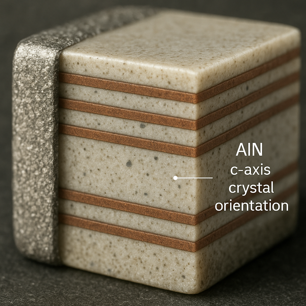
Another key is how the atoms in the material line up. If they all point the same way—what scientists call the “c-axis crystal orientation”—the material works better. Getting this perfect line-up isn’t easy. It depends on what metals you use for the electrodes and how you build the layers.
Past patents and research have shown some success by mixing materials or stacking different metals for the electrodes. For example, using metals like molybdenum (Mo), tungsten (W), or titanium (Ti) can help the dielectric layer line up just right. But getting all these pieces to work together in a real device is still a big challenge.
This is where the new patent steps in. It takes what’s been learned—using doped AlN, controlling the way atoms line up, and smart choices for electrode metals—and puts it all together in one package. The result is a capacitor that is tiny, powerful, and tough enough for the gadgets of tomorrow.
Invention Description and Key Innovations
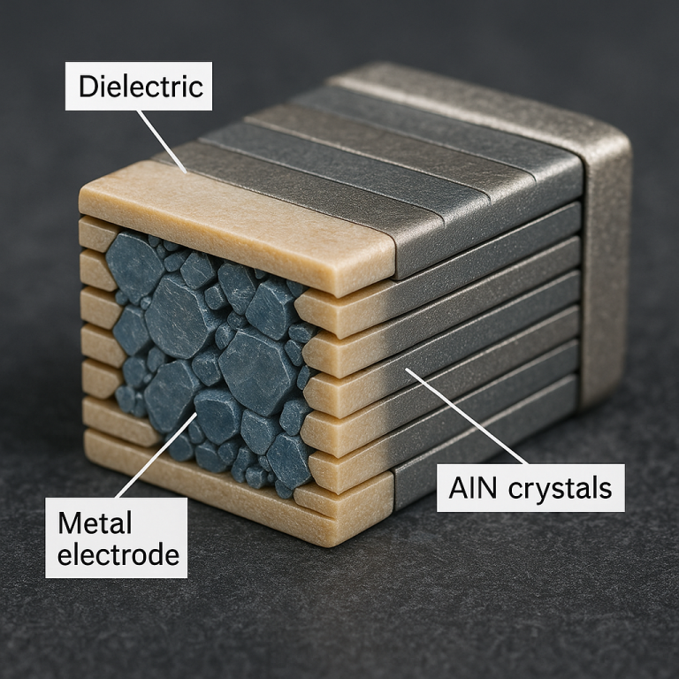
Now, let’s dig into what makes this new multilayered capacitor different and exciting. The heart of the invention is how it uses a special dielectric layer—a thin layer that holds the electric charge.
This new dielectric layer is made from aluminum nitride (AlN), but it’s not just plain AlN. It’s “doped” with other elements like scandium, yttrium, or lanthanum. By carefully adding these elements, the material can hold much more charge. The patent says you should add at least 1% but less than 30% of these elements. Any less, and you don’t get much improvement; any more, and the material gets brittle and hard to work with.
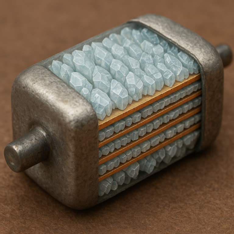
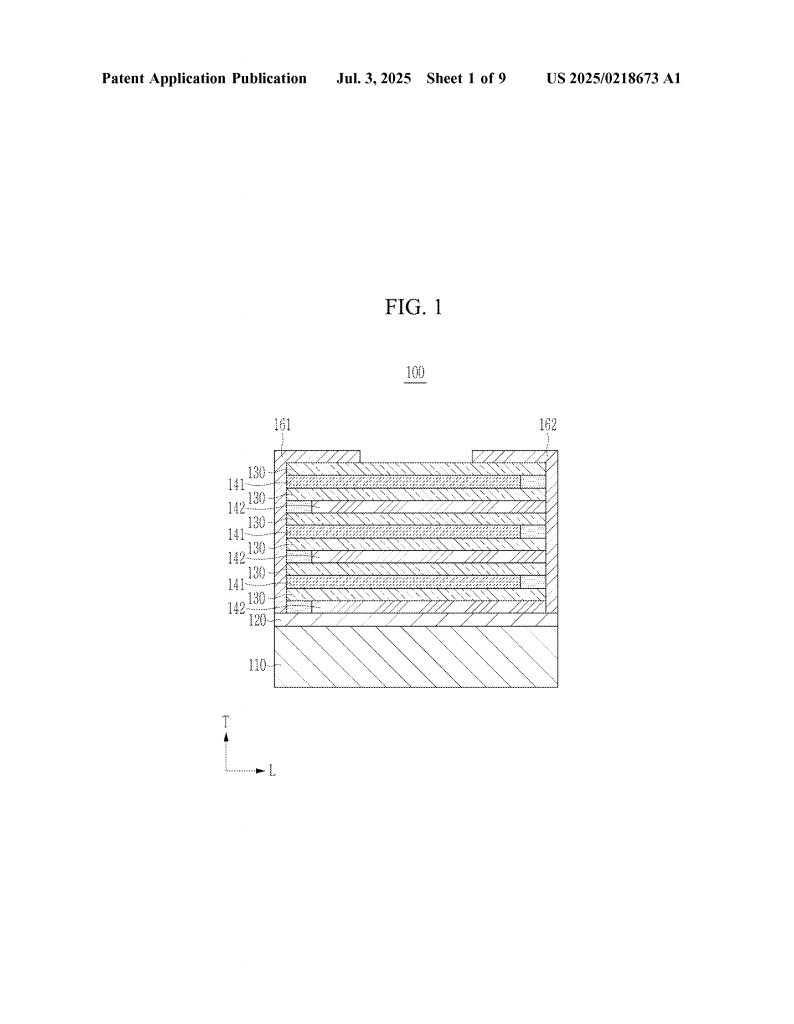
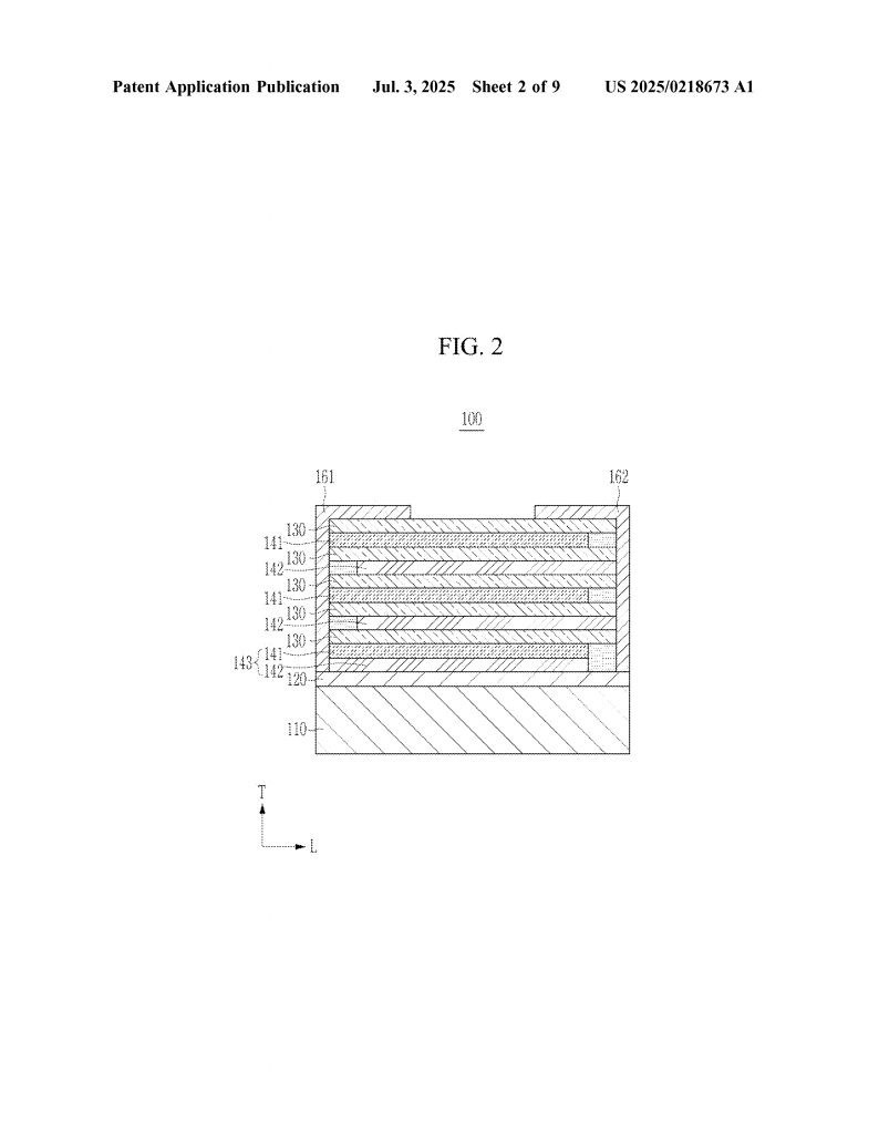
But the real magic is in how the atoms in this layer line up. The patent makes sure that the grains—the tiny crystals that make up the layer—all point in the same direction, called the c-axis. This makes the capacitor very strong and helps it handle high voltages without breaking down. To get this perfect line-up, the patent uses smart choices for the metals in the electrode layers.
For the electrodes, the patent uses metals like molybdenum, tungsten, ruthenium, titanium, platinum, or aluminum. Each of these has a special way that the atoms are packed together (called crystal structure). By matching the way the atoms in the metal and the dielectric line up, the layers can grow together smoothly, like stacking Lego blocks. This keeps the layers thin, strong, and helps the device work even better.
Sometimes, the patent stacks two different metal layers for one electrode. For example, it might use a layer of molybdenum topped with titanium. This double-layer helps the dielectric grow even more perfectly. The layers are made very thin—between 20 and 400 nanometers. For comparison, a human hair is about 80,000 nanometers thick, so these layers are incredibly thin.
The patent also adds a “seed layer” between the base and the capacitor body. This seed layer acts like a starting point, helping all the other layers grow in the right direction. It’s usually made from the same doped AlN material as the dielectric. This extra step makes sure everything lines up perfectly, which boosts performance even more.
Outside the stack of layers, there are external electrodes. These connect the inside of the capacitor to the outside world. They use strong metals like copper or nickel, and sometimes add a resin layer to make them tough and durable. This makes the whole part last longer and work better in tough conditions, like inside a car or a network server.
The way this capacitor is built is also special. The patent describes a way to lay down each layer using precise methods like sputtering or atomic layer deposition. After stacking the layers, special etching and patterning steps create the final shape. This careful building process is key to making sure the layers stay thin and perfect, with no flaws that could cause problems later.
In real-world tests described in the patent, these new capacitors showed much better performance than older types. When scandium was added to AlN, the dielectric constant—the measure of how much charge the material can hold—increased a lot. The right mix of metals and the use of a seed layer made the layers line up just right, further improving performance and reliability.
All these ideas—using doped AlN, matching the crystal structures of the layers, stacking metals, and using a seed layer—work together to create a capacitor that is small, holds a lot of charge, can handle high voltages, and is tough enough for modern electronics. This is a big step forward from what’s been possible before.
Conclusion
The world of electronics is moving fast. Devices are getting smaller, smarter, and more powerful. To keep up, the tiny parts inside them, like capacitors, need to get better too. This new patent shows a clever way to make capacitors that are stronger, can hold more charge, and last longer, all while staying tiny. By using special materials, making sure the layers line up perfectly, and building everything with care, this invention could help power the next generation of gadgets, cars, and networks. If you work with electronics or just love new technology, this is a development to watch closely.
Click here https://ppubs.uspto.gov/pubwebapp/ and search 20250218673.