IMAGE SENSING DEVICE
Invented by CHO; Min Su
Image sensors are everywhere. They are in your phone, your car, your computer, and even in your home security cameras. With technology growing so fast, these sensors have to keep up. Today, we are going to explore a new and exciting patent application for an image sensing device that uses two special meta-lens layers. Let’s look at where this idea fits in the market, what science and old inventions came before, and what makes this new invention stand out from the rest.
Background and Market Context
Digital cameras and image sensors have become a big part of our lives. Almost every device you use has some way to see the world, from your smartphone’s camera to tiny sensors inside cars that help with parking or safety. These sensors work by turning light into electronic signals, which are then used to make pictures or to help smart machines make decisions.
The need for better, smaller, and faster image sensors keeps growing. People want sharper photos, even in low light. Cars need sensors that work in bright sunlight and at night. Doctors use small cameras for surgery. Even robots and computers rely on sensors to “see” and understand their surroundings. This means companies are always trying to make image sensors that are more sensitive, use less power, and fit into smaller spaces.
Traditionally, image sensors have been made using two main types of technology: CCD (charge-coupled device) and CMOS (complementary metal-oxide-semiconductor). Both have their strengths, but CMOS sensors are now more popular because they are cheaper and easier to put into small gadgets. Still, as we shrink these sensors, making each pixel smaller, problems start to show up. When pixels get too tiny, they do not catch as much light, which can make pictures look dark or noisy.
Another challenge is making sensors that can see different colors (like red, green, and blue) or even infrared light for special uses. This usually means adding extra filters or layers, which can make the sensor thicker and harder to build. The more layers and thickness, the more complicated and expensive the process becomes.
To solve these problems, the market is looking for new ways to shrink pixel size without losing quality. Companies want sensors that work better in low light, are thinner, and cost less to make. This is where the new dual meta-lens image sensor comes in. By using two very thin layers with special nanostructures (tiny shapes built at the scale of atoms), this new design hopes to make image sensors sharper, smaller, and more flexible for all kinds of gadgets.
Scientific Rationale and Prior Art
To really understand the new dual meta-lens sensor, it’s helpful to know what has been tried before and what science makes this possible.
Most image sensors work by using a piece of silicon with many tiny light detectors, called photodiodes. Above these detectors, color filters let only red, green, or blue light through, so the sensor can tell colors apart. Sometimes, special filters are used to block out unwanted light, like infrared, which can mess up pictures.
To make a sensor more sensitive, one simple way is to make the layer that collects light (called the epitaxial or “Epi” layer) thicker. But a thicker layer means a bigger sensor, which can be a problem if you want tiny cameras. More thickness also makes it harder and more expensive to make the sensor, and can cause problems with how the device works.
Another trick has been to use microlenses. These are like tiny magnifying glasses placed over each pixel to help focus more light into each photodiode. This helps, but as pixels get smaller, even microlenses start to lose their magic because the distance the light has to travel is so short. The lenses themselves also take up space and add to the thickness of the sensor.
Recently, scientists have started using something called “meta-lenses.” These are ultra-thin surfaces covered with tiny structures, often made of silicon or other materials, that bend and focus light in special ways. Instead of using a curved shape like a normal lens, meta-lenses use the way light interacts with these tiny shapes to do the same job, or even better. They can be much thinner than regular lenses and can be designed to focus different colors of light to different places.
There have been patents and research on using a single meta-lens layer to focus light onto image sensors, making them thinner and more efficient. Some designs have used special coatings or mirrors under the sensor to reflect lost light back into the detector, trying to boost sensitivity. But each of these ideas has limits. A single meta-lens can only do so much, and coatings or mirrors tend to reflect all colors the same way, which can cause mixing and reduce picture quality.
What hasn’t been done before is using two separate meta-lens layers — one above and one below the sensor — each designed to work with light in its own way. By carefully shaping both layers, it becomes possible to catch more light, keep colors clear, and make the sensor thinner than ever before. This idea also opens up new ways to use the sensor for infrared light, which is important for things like face recognition or night vision.
So, while microlenses and meta-lenses have been used before, putting two different meta-lens layers in a sensor, each with a unique job, is a new step forward. This approach combines ideas from optics, nanotechnology, and semiconductor science to solve the problems of thin, high-quality image sensors.
Invention Description and Key Innovations
This new patent describes an image sensor with a special layered structure. At its heart, the invention stacks its parts in a way that makes the most out of every bit of light, while keeping the sensor thin and easy to build. Here’s how it works:
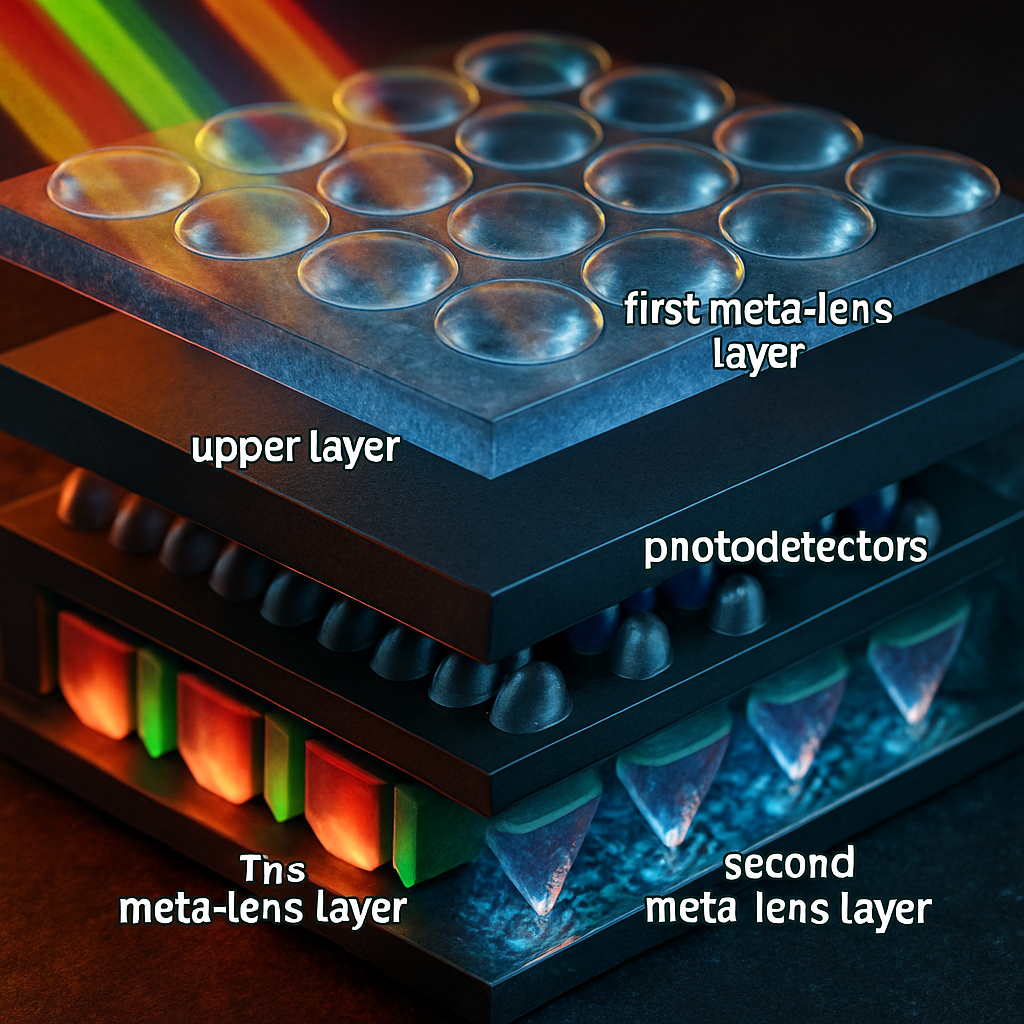
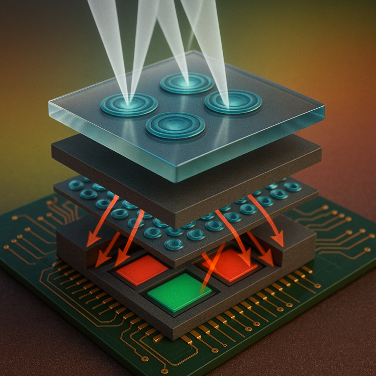
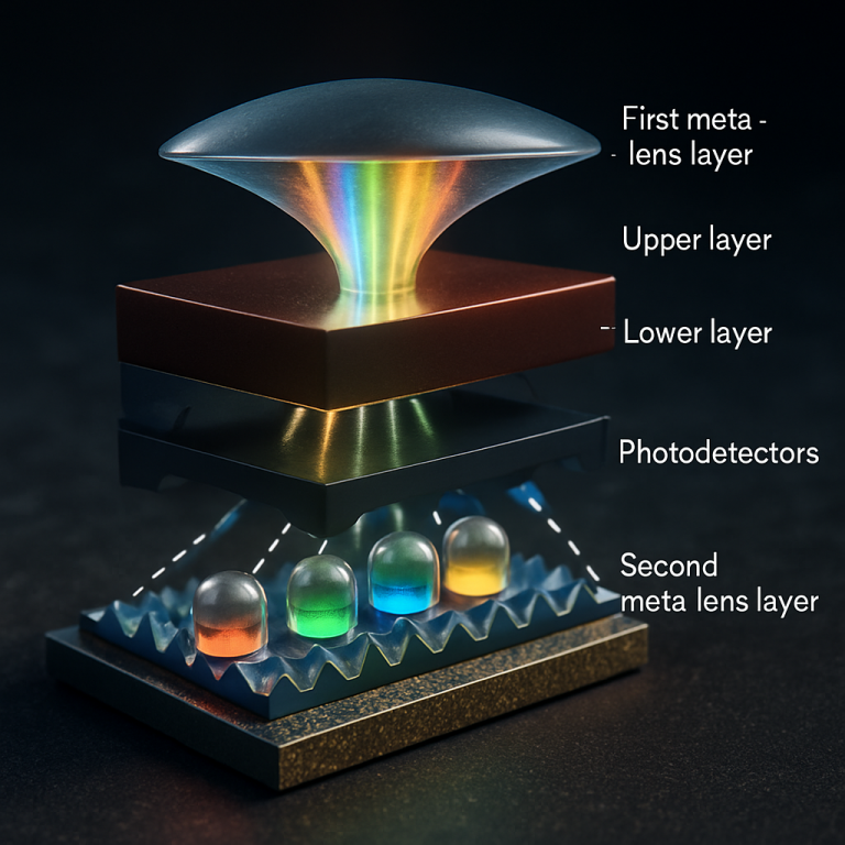
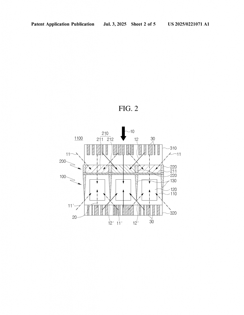
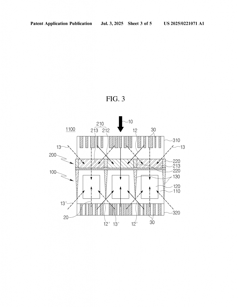
The sensor has a lower layer made from a silicon base. This layer holds many tiny light detectors, called photodetectors or photodiodes. These are the parts that turn light into electric signals. Between the photodetectors, there are special isolation regions. Think of these as tiny walls that keep each detector from mixing signals with its neighbors, which helps keep the picture sharp and colors true.
On top of this lower layer sits an upper layer. This upper layer can have color filters (for red, green, and blue) or infrared filters, depending on the type of sensor. These filters let only certain colors or types of light reach each photodetector. To keep each color separate, more isolation regions are placed between the filters.
Now, here’s where the invention gets really clever. Over the very top of the sensor is the first meta-lens layer. This layer is made from nanostructures — patterns so small they are built atom by atom. These tiny shapes act like a super-thin lens, bending and focusing light in special ways. The meta-lens can be designed so that red light is focused right onto the red filter, green onto the green, and blue onto the blue. This means more of the right color of light gets to each pixel, making the sensor more sensitive and the colors richer.
The magic doesn’t stop there. Under the bottom of the sensor, there’s a second meta-lens layer. Instead of focusing light, this lower meta-lens is built to scatter or reflect light that passes through the sensor. Instead of letting this light escape and go to waste, the layer bounces it back up into the photodetectors. By carefully shaping the nanostructures in this layer, the sensor can direct different colors of light back to exactly the right spot, boosting sensitivity even more.
This setup creates a kind of “cavity resonance” — a space where light can bounce back and forth in just the right way to be absorbed better by the photodetectors. The inventors can make the sensor thinner by reducing the thickness of the Epi layer, since the dual meta-lens system makes sure almost all the light gets used. The upper and lower meta-lens layers can also be made with different materials or shapes, so they each handle light in their own special way.
There are other nice features, too. The sensor can be built with or without color filters, allowing it to work for normal color cameras or for infrared cameras, just by changing the upper layer. This flexibility means the same basic design can be used in lots of different products, from phone cameras to car sensors to medical devices.
Another key point is that the meta-lens layers are very thin. They add hardly any thickness to the sensor, which helps keep production simple and costs down. The nanostructures can be made using the same types of manufacturing steps used for other parts of the sensor, so companies can use existing factories and equipment.
By using two different meta-lens layers, this invention solves the biggest problems facing image sensors today. It makes pixels more sensitive, even when they are tiny. It keeps sensors thin, so they can fit into slim devices. It can be adapted for both normal color and infrared sensing. And it does all this without adding much cost or complexity to the manufacturing process.
Conclusion
The dual meta-lens image sensor is a big step forward for digital imaging. By stacking two different nano-lens layers above and below the sensor, this design catches more light, keeps images sharp, and allows for thinner, more flexible sensors. This means better pictures and smarter devices, all in smaller packages. Whether for phones, cars, medical tools, or robots, this invention opens the door to new uses and better performance everywhere image sensors are needed. Watch for this technology to become a standard in the next generation of digital cameras and smart devices.
Click here https://ppubs.uspto.gov/pubwebapp/ and search 20250221071.