Headline: Faster, Smarter Data Flow for Semiconductor Devices Boosts Memory Performance in Computing Systems

Invented by KA; Dong Yoon, PARK; Min Cheol, SK hynix Inc.
Memory chips are the brains behind every smart gadget you use. But as devices get faster, moving data in and out of these chips gets harder. Errors can sneak in, especially as we push for higher speeds and smaller chips. Today, we’ll walk through a new memory device patent, digging into how it aims to make data safer and chips more reliable. If you’re curious about how memory chips work and want to understand a real-world patent at a simple level, you’re in the right place.
Background and Market Context
Memory chips are everywhere. They help your phone store pictures, your laptop run programs, and your car remember how to drive. Every year, companies make chips faster and smaller. This helps your devices do more, but it brings new problems. As chips move data faster, even tiny errors can cause big troubles—like freezing your phone or losing your work.
Think about how fast memory works now. Newer standards like DDR4 and DDR5 can move lots of data every second. That’s great for speed, but it means there’s less room for mistakes. Even the smallest hiccup—a tiny electrical glitch or a tired wire—can flip a bit from 0 to 1 or vice versa. That can mean a wrong number in your spreadsheet, a corrupt photo, or a system crash.
Chipmakers know this. They spend lots of time and money finding ways to catch and fix these errors. They use tricks like error correction codes (ECC) and build-in spare pieces called “redundancy” that can step in if something breaks. But as chips keep shrinking, it gets harder to keep everything perfect.
That’s why the market for better, safer memory is big and growing. Big companies need servers that don’t crash. Gamers want computers that run fast and smooth. Cars, robots, and even medical devices need memory that never fails. If you can make a memory chip that’s both quick and tough, you’ve got something valuable.
The patent we’re looking at today is about making memory chips not only faster but also more reliable. It tries to balance the need for speed with the need for safety, using clever ways to move, block, and repair data inside the chip. This invention could help make the next generation of gadgets smarter and safer.
Scientific Rationale and Prior Art
Let’s break down why this invention matters and what came before it.
When you look inside a memory chip, you see lots of little boxes called “mats.” Think of them as tiny rooms where data is stored. Each mat holds part of your information. When you want to read or write data, the chip decides which mats to use and which parts inside those mats to touch. This is done using signals called “addresses” and “column signals.”
In the past, chips would just move data in and out, hoping nothing goes wrong. But as chips got faster, errors happened more often. To help, engineers started using error correction codes (ECC). These are like secret checks that can spot and sometimes fix mistakes in the data. They also added extra columns, called “repair column lines.” If one part breaks, a repair column can take over.
Another idea is to use “meta regions.” These are special parts of the chip that can store extra info, like error codes or backup data. In some chips, these regions only hold error info. In others, they can also help store real data if needed.
Older patents and products use these ideas, but they have limits. For example, many just block or repair data at the whole mat level, not at the smaller column level. Some chips can’t switch easily between using meta regions for error info and using them for real data. Others struggle to keep up as data speeds grow.
This new invention builds on all those ideas. It combines error correction, spare columns, and flexible meta regions in new ways. It can block or fix just one part of the data, not the whole thing. It uses smart signals (called flag, mask, and shift signals) to control which data gets through, which gets blocked, and which gets repaired. It can also change how the meta region is used, depending on what the chip needs at that moment.
This means the chip can fix problems on the fly, keep data flowing even when something breaks, and use every part of the chip in the smartest way possible. That’s a big step up from older designs, which were often less flexible and less able to handle the fast pace of modern gadgets.
Invention Description and Key Innovations
Now let’s dive into what this new patent actually claims and how it works.
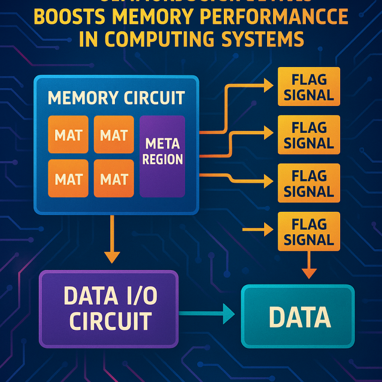
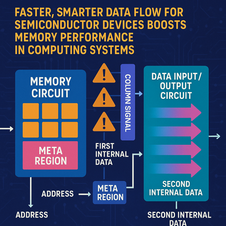
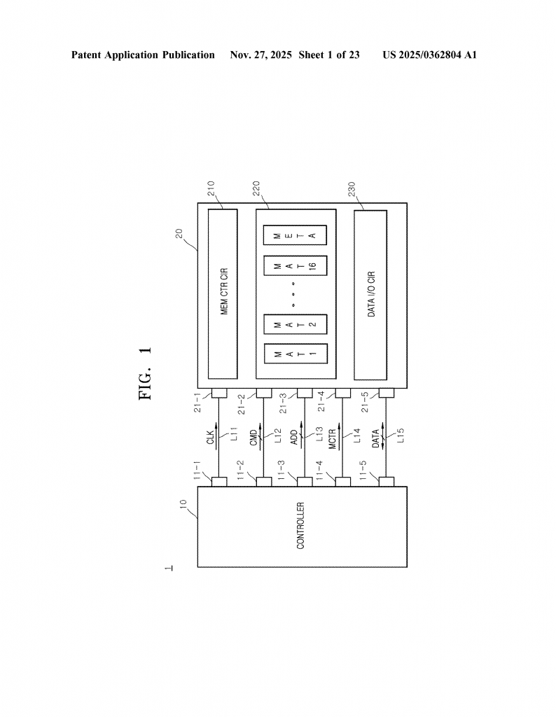
At the heart of the invention is a memory chip made up of several mats and a special meta region. Each mat is like a little storage room, and the meta region is a kind of “VIP room” that can hold special data, like error information or backup copies.
Here’s how the magic happens:
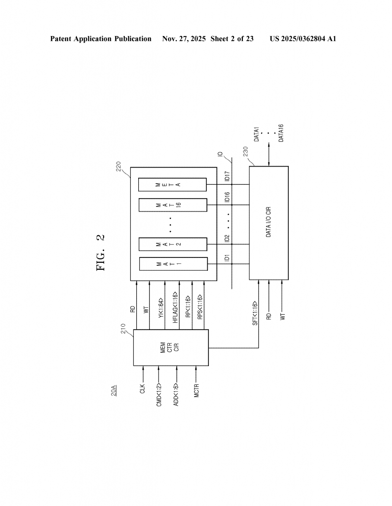
When the chip gets a command to read or write data, it uses a smart control circuit to decide how to handle each piece of information. The control circuit looks at the address (where the data should go), checks if anything is broken, and then sends out signals to tell the mats and the meta region what to do.
If everything is normal, the chip moves data in and out of the mats as usual. But if there’s a problem—like a broken column inside a mat—the chip can block that part, use a repair column instead, or send the data to the meta region for safekeeping.
The chip uses several types of signals to manage this:
1. Flag signals: These are like traffic lights. If a flag is “on,” it means a certain part of the mat should be blocked (no data in or out). This helps keep bad data from spreading.
2. Masking and shifting signals: These help the chip re-route data. If a certain part should be skipped or replaced, the chip uses these signals to shuffle the data around, so the right information ends up in the right place.
3. Repair signals: If the chip knows a certain column is broken (maybe from a factory test or from use), it can switch in a spare “repair column” to take over. This happens automatically, without stopping the chip or losing data.
4. Meta control signal: This tells the chip when to use the meta region for error info or for holding regular data. If an error is detected, the meta region can store special codes that help find or fix the problem later.
The meta region is especially clever. In normal mode, it can help with error checking or hold backups. In “meta mode,” it can store or supply real data just like a regular mat. The chip can block certain parts of the meta region if needed, so only safe data gets through.
The chip also uses a special circuit to select and move data. Think of it like a group of tiny switches (called multiplexers) that pick the right data to send out, based on the signals mentioned above. If one data path is blocked or broken, the switch picks another, so the chip keeps running smoothly.
All this happens very fast, every time you read or write data. The chip can even repair itself on the fly, swapping in spare columns without stopping. If a problem is found, the chip can block the bad data, use the meta region for help, and send the right data to the outside world—all in a single clock cycle.
This design means the chip is both tough and flexible. It can handle errors without stopping, use every part of the chip to the fullest, and keep your data safe even as speeds go up and chips get smaller.
Conclusion
This new memory chip invention is all about making data safer and chips more reliable. By using smart signals, flexible meta regions, and self-repair features, it lets memory chips keep up with the demands of today’s fast, always-on world. Errors are caught and fixed without slowing down, and the chip can adapt to problems on the fly. For anyone who wants faster, tougher gadgets—from phones to servers to cars—this kind of technology is the future. As chips get smaller and more powerful, these smart designs will be key to making sure our data is always safe and ready when we need it.
Click here https://ppubs.uspto.gov/pubwebapp/ and search 20250362804.