Boosting Memory Chip Reliability with Automated Fault Detection and Self-Repair Technology
Invented by BAEK; Seungbum, PARK; Sungcheol, Samsung Electronics Co., Ltd.
Let’s dive into how memory chips are getting much smarter at fixing themselves and why that matters for everything from your phone to giant data centers. This article unwraps a new patent that teaches memory chips how to spot and repair weak spots all by themselves, so your data stays safe and your devices work better, longer. We’ll walk through what’s happening in the memory world, the science behind the invention, and the smart ideas that make this patent special.
Background and Market Context
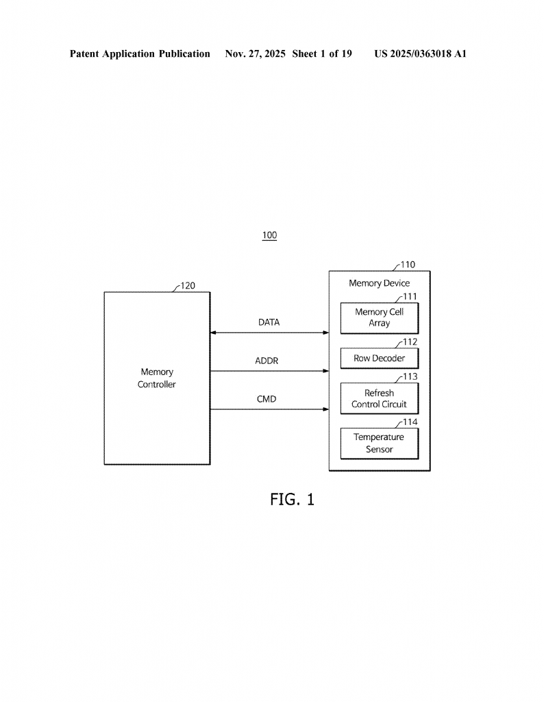
Memory chips are everywhere. They live inside your smartphone, power your laptop, and keep cloud servers running 24/7. These chips store all the data that makes your apps, games, and online tools work. But making memory chips is hard work — the tiny parts inside can get damaged or wear out over time, especially as chips get smaller and more powerful.
When even one memory cell — a spot where a single bit of data lives — gets weak, it can cause big problems. These weak cells might lose data faster than others, or just stop working altogether. If too many cells go bad, your device might crash, slow down, or lose data. Manufacturers have long used “redundancy” to help — extra cells are built in so they can step in if a cell fails. But figuring out exactly when and how to use those spares has always been tricky.
The market for memory chips is huge and only growing. Cloud computing, artificial intelligence, and always-on devices all depend on reliable, fast memory. When memory fails, it can cost money, time, and trust. This is why companies pour billions into making memory more reliable. Still, as chips get more complex, it’s harder to keep every cell working perfectly.
A big problem is the “refresh period.” In most modern memory, especially DRAM, data can fade unless it’s refreshed regularly. Designers have to set the refresh rate based on the weakest cell, which means the whole chip might refresh more often than needed — wasting power and slowing things down. If you could find and repair those weak cells, you could make the chip faster and save energy.
This patent answers that call. It brings a new way for memory chips to test themselves, spot the weak cells, and swap them out for better ones — all automatically, and even as the chip ages or heats up. That means longer-lasting, more reliable memory, with less wasted work. In a world that needs more data, faster, and with less waste, this is a big leap forward.
Scientific Rationale and Prior Art
To understand what’s new here, let’s look at how memory repair has worked before, and why those old methods aren’t good enough anymore.
Traditionally, memory chips come with extra “redundant” cells. If a chip tester finds a bad cell during production, the chip is programmed to use a spare cell instead. This “repair” is usually done once, right after the chip is made. After that, the chip doesn’t check again — so if another cell goes bad later, there’s not much that can be done.
Some systems use “error correction codes” (ECC) to spot and fix small errors as they happen. ECC can fix data mistakes, but doesn’t actually repair the cell itself. And as chips shrink, errors become more likely, and ECC alone can’t keep up.
A few advanced memory systems can do “post-package repair,” where chips are retested after being put into modules. This is better, but still not enough. Most repair happens only at the factory, not in real time as the chip is used. Memory cells can get weaker over time — from age, heat, or other stresses. If a chip can’t check itself and repair on the fly, it risks failure in the field.
Researchers have looked at ways to measure “retention time,” or how long a cell can hold data before it fades. Some systems can find the weakest cells and adjust the refresh period, but this usually means all cells are refreshed more often, which is wasteful. Some ideas use “adaptive refresh,” where only weak areas are refreshed more, but they still don’t repair the cells themselves.
What’s been missing is a way for the chip to regularly test each cell, figure out exactly which are weak, and repair them automatically, even after the chip leaves the factory. Prior patents and systems don’t combine all these features in one, and few are designed to respond to changes like rising temperature or cell aging over time. That’s where this new patent steps in.
Invention Description and Key Innovations
Now let’s get to the heart of the invention — a memory system that is always watching itself, smartly fixing weak spots, and adjusting as conditions change.
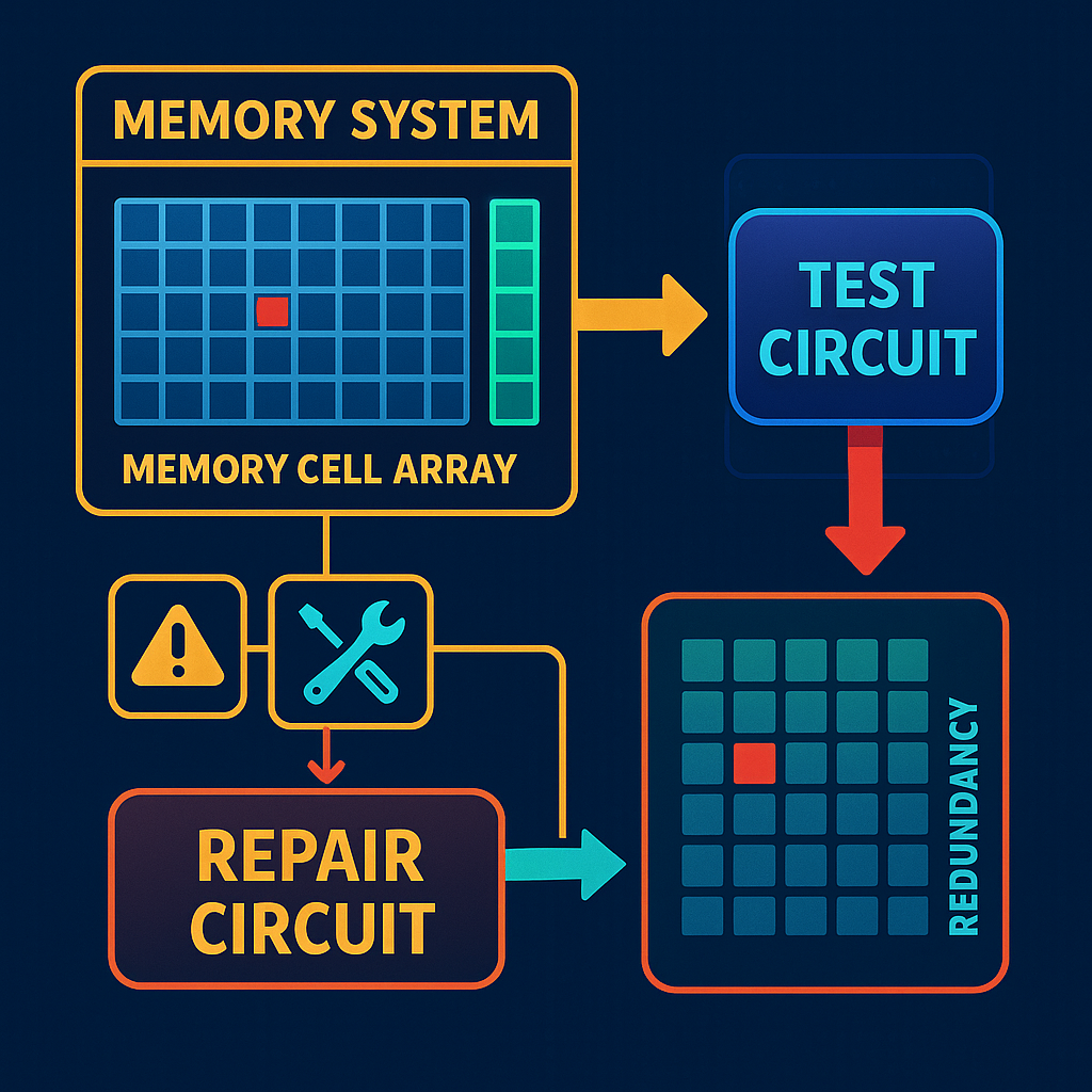
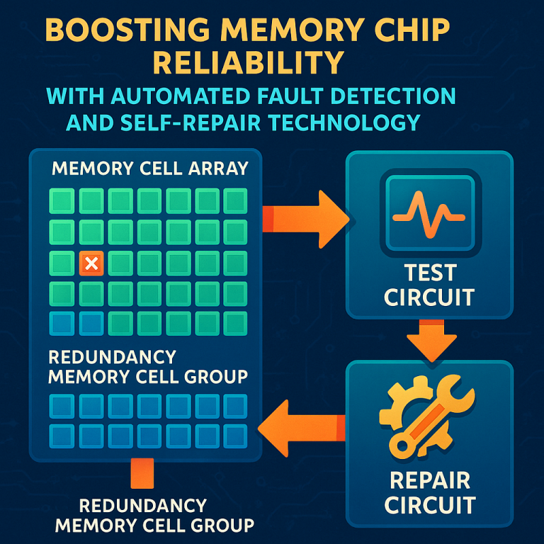
At its core, this memory system is built from three main parts:
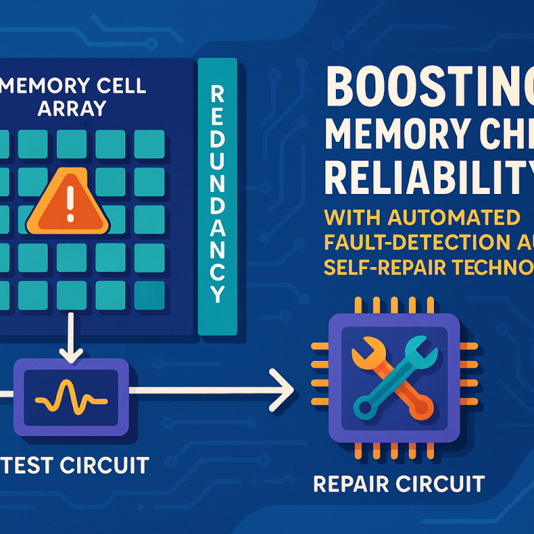
- A memory cell array, which holds regular memory cells and a group of extra, redundant cells.
- A test circuit, that regularly checks each cell to see how long it can hold data (its “retention time”).
- A repair circuit, that steps in to swap out weak cells with healthy spare cells when needed.
Here’s how it works in simple terms:
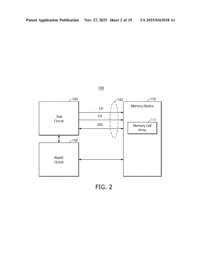
Every cell in the memory array is checked by the test circuit. The test writes a bit (say, a 1 or 0), waits for a set period, and then reads it back. If the bit has changed, it means the cell couldn’t hold its data long enough — its retention time is too short. The circuit checks each cell this way, both for ones used in normal operation and for the spare (redundancy) cells.
The system keeps track of which cell has the shortest retention time. If any cell falls below a safe level (set by a “preset refresh period” or a chosen threshold), the repair circuit is triggered. This circuit picks one of the good spare cells — only if it has a longer retention time than the weak cell — and reroutes data so the spare cell takes over.
If many weak cells are found, the system can repair them one by one, starting with the weakest. The repair isn’t limited to single cells — if needed, it can swap out whole rows, columns, or even groups of cells, depending on how the memory is organized. The process is flexible, and can be done during manufacturing, after packaging, or even later when the chip is in use.
A key innovation here is that repairs are not just one-time events. The test circuit can run again and again, even as the chip ages or as temperature rises. For example, if the chip gets hot (which makes data fade faster), a temperature sensor tells the controller to check cells more often, or to tighten the rules for what counts as “weak.” If repairs are made, the controller can adjust the refresh period, making the chip run more efficiently.
Another clever point is how the retention time is measured. The system uses both 1s and 0s, since some cells might leak faster for one value than the other. By testing both, it finds the real weakest point. The process is careful and smart — it narrows down the exact moment a cell “flips” by adjusting the wait time for each test, so it gets a true picture of how strong or weak each cell is.
The patent also covers how this approach fits into real memory packages, like stacked memory used in high-end graphics cards or AI servers. There are options for direct test and repair access, so chips can be checked and fixed without even needing to run through the main processor. This makes it easier to service memory before it’s sent to customers or even after it’s built into bigger systems.
In short, this invention brings together a set of smart, practical steps:
- Tests every cell, both regular and spare, for real retention time under real conditions.
- Repairs weak cells on the fly, using only spare cells that are proven to be better.
- Responds to changing conditions, like rising temperature or chip aging, adjusting the refresh rate or repair threshold as needed.
- Works at many levels — from single cells to whole groups — and fits into both everyday and high-end memory chips.
- Improves data safety, lets memory run faster and longer, and helps save energy by avoiding wasteful refreshes.
These steps are tightly connected and work together in a loop: test, compare, repair, adjust, and repeat. It’s a smart, flexible, and forward-looking way to make memory chips tough enough for the demands of today and tomorrow.
Conclusion
The new memory system described in this patent is a leap forward in how chips protect your data and keep running strong. By letting memory chips test themselves, spot weak spots, and smartly repair them with proven-good spare cells, this invention solves big real-world problems. It means your devices will last longer, run faster, and waste less energy — all while keeping your data safe, even as things heat up or wear down.
This approach is not just smart, it’s necessary. As our world leans more on data, and as chips get smaller and more complex, memory needs to be both tough and clever. This patent shows a way to get there, with ideas that are actionable for chip makers and valuable for everyone who depends on digital devices. If you care about the future of reliable, efficient, and self-healing memory, this is a technology to watch.
Click here https://ppubs.uspto.gov/pubwebapp/ and search 20250363018.