AMPLIFICATION CIRCUIT, AND RECEIVER CIRCUIT AND SEMICONDUCTOR APPARATUS USING AMPLIFICATION CIRCUIT
Invented by CHOI; Sung Phil, SK hynix Inc.
In today’s world, chips are everywhere—from phones to cars. These chips need to quickly and accurately read signals. One of the newest ideas to help chips read signals better is a special kind of amplification circuit. This article explains what problem this new circuit solves, why it matters, and how it works in a way anyone can follow.
Background and Market Context
Chips, or semiconductor devices, are at the heart of all modern electronics. They control everything from computers and smartphones to cars and TVs. One of the main jobs of these chips is to read signals. These signals can be very weak and can easily get mixed up with noise, which makes it hard for the chip to know what the signal really means. This is where amplification circuits come in—they make weak signals stronger so the chip can read them clearly.
As chips are made smaller and smaller, new problems appear. Tiny parts inside the chip can act like small unwanted capacitors. These are called parasitic capacitors. They can cause something called “kickback noise,” which is like an echo that makes it hard for the chip to know if it is reading the real signal or just noise. This can cause errors, especially when the chip is running very fast or when the signals are very weak.
In the past, engineers tried to fix these problems by adding more parts to the circuit or by slowing down the chip. But people want faster, smaller, and more reliable electronics. So there is a real need for a better way to get clean, strong signals inside chips, even as they get smaller and more complicated. This is important not just for phones and computers, but for things like self-driving cars, medical devices, and smart home gadgets.
The market for chips is huge and keeps growing. Every company making electronics wants their devices to be faster and use less power. They also want them to work well in all kinds of situations, from very hot to very cold, or when the power supply is not perfect. So, any new way to make chips more reliable and accurate, especially when reading signals, is a big deal. It can help companies make better products and can even open up new markets.
This is why a new kind of amplification circuit, like the one in this patent application, is so important. It promises to help chips read signals more accurately, even as the parts inside the chip get smaller and more affected by noise.
Scientific Rationale and Prior Art
To understand why this new circuit is special, let’s look at how chips usually read signals and what problems they face.
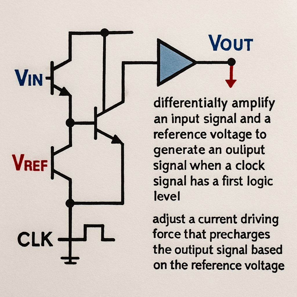
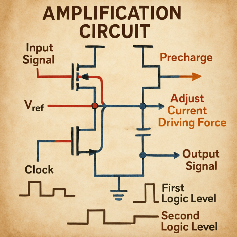
When a chip reads a signal, it usually compares two voltages: the signal itself and a steady “reference” voltage. The difference between these two tells the chip if it should read a 1 or a 0. This is called differential amplification. The circuit that does this is called an amplifier.
But there’s a problem. Inside the chip, the wires and parts are so close together that they start to affect each other. When one part changes voltage quickly, it can cause unwanted changes in another part. This is the “kickback noise” mentioned earlier. It makes the amplifier think the signal changed, when actually it’s just noise from another part of the chip. This reduces the “sensing margin”—the space the amplifier has to decide if it’s seeing a real signal or just noise.
Older solutions tried to fix this by making the amplifier bigger, adding filters, or using extra circuits to remove the noise. But bigger circuits use more power and space, and filters can slow down the chip. Some designs tried to precharge the amplifier’s output nodes (the parts that give the final signal) to a certain voltage before reading a new signal. This helps, but only if the precharge is just right. Too much or too little, and it can cause new problems.
Other patents and designs have explored ways to control the precharge current—how much energy is used to set up the amplifier before it reads. Some used fixed settings, others tried to adjust based on the clock signal (the heartbeat of the chip). But none of them could easily react to changes in the reference voltage, or adjust quickly if the signal conditions changed.
As chips get smaller and run at lower voltages, these problems get worse. The noise gets bigger compared to the signal, and small errors can cause the chip to make mistakes. So, the need for a smarter, more flexible way to control the amplifier and its precharge current is very real.
This patent application builds on these earlier ideas but adds something new. It proposes a way for the amplifier to watch the reference voltage and adjust how hard it precharges the output. This sounds simple, but it means the amplifier can quickly react to changes and keep the sensing margin big. That way, the chip can read signals more accurately, even if the voltage or noise changes.
Invention Description and Key Innovations
Now, let’s break down how this new amplification circuit works, and what makes it different from what came before.
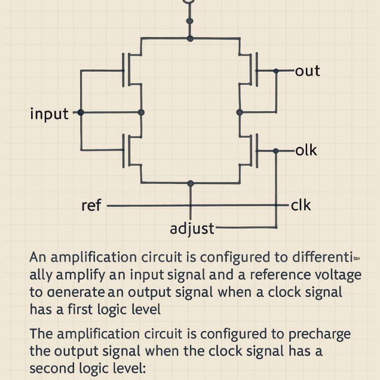
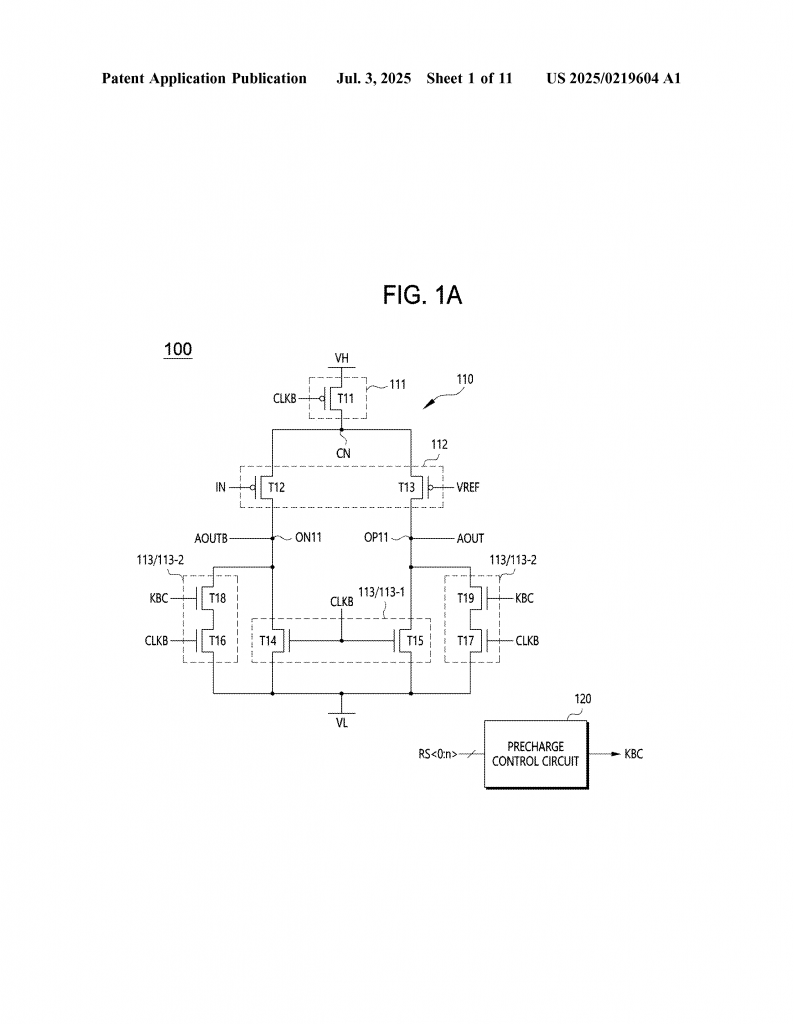
At its heart, this invention is an amplifier circuit with a special control system for the precharge phase. The main parts are:
1. A precharge control circuit that looks at the reference voltage and decides how much current to use during precharge.
2. An amplifier that both amplifies the difference between the input signal and the reference voltage, and precharges its output nodes to a set voltage.
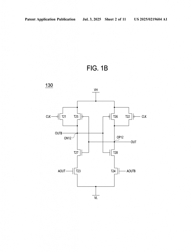
3. Extra parts, like latches, to hold the signal steady after it’s read.
Here’s how it works in simple steps:
When the chip is ready to read a new signal, the amplifier waits for a clock signal. When the clock says “go,” the amplifier compares the input and the reference voltage. It makes the output nodes move up or down, showing if it read a 1 or a 0.
But before each reading, the amplifier “precharges” its output nodes to a certain voltage. Think of this like resetting a scale to zero before you weigh something. If you don’t reset, you might get the wrong answer. The precharge control circuit decides how much current to use during this reset based on the current reference voltage.
If the reference voltage is high, the circuit may use more current to precharge quickly and overcome more noise. If the reference voltage is low, it uses less current, which saves power and avoids overdriving the nodes. This is all automatic and adapts in real-time.
The circuit can use either P-type (PMOS) or N-type (NMOS) transistors, depending on what works best for the chip. It can also use two amplifiers working in turn—while one reads, the other precharges. This helps the chip handle signals even faster.
The design includes specific control paths so the precharge can be fine-tuned using a control signal, which itself comes from either directly sensing the reference voltage or from a signal that tells what the reference voltage will be. The control circuit compares this signal to a threshold, and then enables or disables extra precharge current as needed.
All this means the circuit can keep the sensing margin big, even if noise or voltage changes. It also means the chip can run faster and still read signals accurately. It can be used in memory chips, CPUs, or any system where fast, accurate signal reading is needed.
Another smart feature is the use of latches after the amplifier. When the amplifier reads a signal, the latch holds that value steady, so the rest of the chip can use it. The latch also uses a smart precharge system, so it is always ready for the next signal without errors or delays.
In a bigger system, like a computer or a phone, this circuit can be used in the parts that read and write data. For example, in memory chips, it helps make sure the right data is read every time, even as voltages and noise change. It also helps save power by using only as much precharge current as needed, and no more.
By making the amplifier and precharge system smarter and more flexible, this invention helps chips keep up with the demand for faster, smaller, and more reliable electronics. It also means that future chips can be even smaller, since the amplifier can handle more noise without getting bigger.
The circuit is simple enough to fit into modern chip designs but smart enough to make a real difference in performance and reliability.
Conclusion
Chips are getting smaller and faster every year, but the problem of noise and accurate signal reading is getting harder. This new amplification circuit solves a big part of that problem by making the precharge phase smarter and more adaptable. By watching the reference voltage and adjusting the precharge current automatically, it makes sure the chip always has a clear, strong signal to read. This leads to better performance, lower power use, and fewer errors. For anyone designing chips for the next generation of electronics, this kind of innovation is key. It keeps technology moving forward and helps make all our devices work better.
Click here https://ppubs.uspto.gov/pubwebapp/ and search 20250219604.