Next-Gen Semiconductor Design Boosts Efficiency and Performance for Advanced Electronics Manufacturers
Invented by KIM; Kang Lib, LEE; Dongjin, LEE; Jaeduk
The world of electronics changes quickly, and the latest advances in memory chips are no exception. In this article, we break down a newly published patent application for a stacked semiconductor device that promises to take memory storage to the next level. We will walk you through the background of this technology, look at what science and inventions came before, and then explain the inventive ideas that make this new chip stand out. Let’s dive right in.
Background and Market Context
Today, nearly every device in our lives—phones, computers, even cars—relies on semiconductor memory. These chips are responsible for storing all the data and programs that make our digital world possible. But as we use more data and want faster, smaller gadgets, the demand for better, more powerful memory chips keeps growing.
In the past, most semiconductor memory chips were built in a flat, two-dimensional way. Imagine a tile floor—each tile is a memory cell, and they all sit side by side. This worked well for a while, but as the need for more memory grew, chip makers ran out of room. You can’t make the tiles much smaller without running into problems, like electrical interference or defects during making.
To solve this, the industry moved to three-dimensional (3D) structures. Think of stacking tiles into towers instead of just spreading them out. Now, you can fit many more memory cells into the same chip area by building up instead of out. This is called “3D NAND” or “vertical NAND.” With 3D memory, smart gadgets could store more photos, apps, and videos without needing bigger chips.
But even 3D memory has its limits. As companies try to pack more and more cells into each chip, the space between important parts gets tighter. If you make things too close together, it becomes hard to control the chip’s behavior during manufacturing. Problems like short circuits or unreliable connections become more common. This is where the new patent comes in—it introduces a better way to make connections inside these stacked chips, allowing for even greater storage without the usual risks.
As demand for faster, smaller, and cheaper memory continues, companies are racing to find new ways to overcome these challenges. Whoever solves these problems first will be able to offer better performing chips at lower costs, a huge advantage in the competitive electronics market.
Scientific Rationale and Prior Art
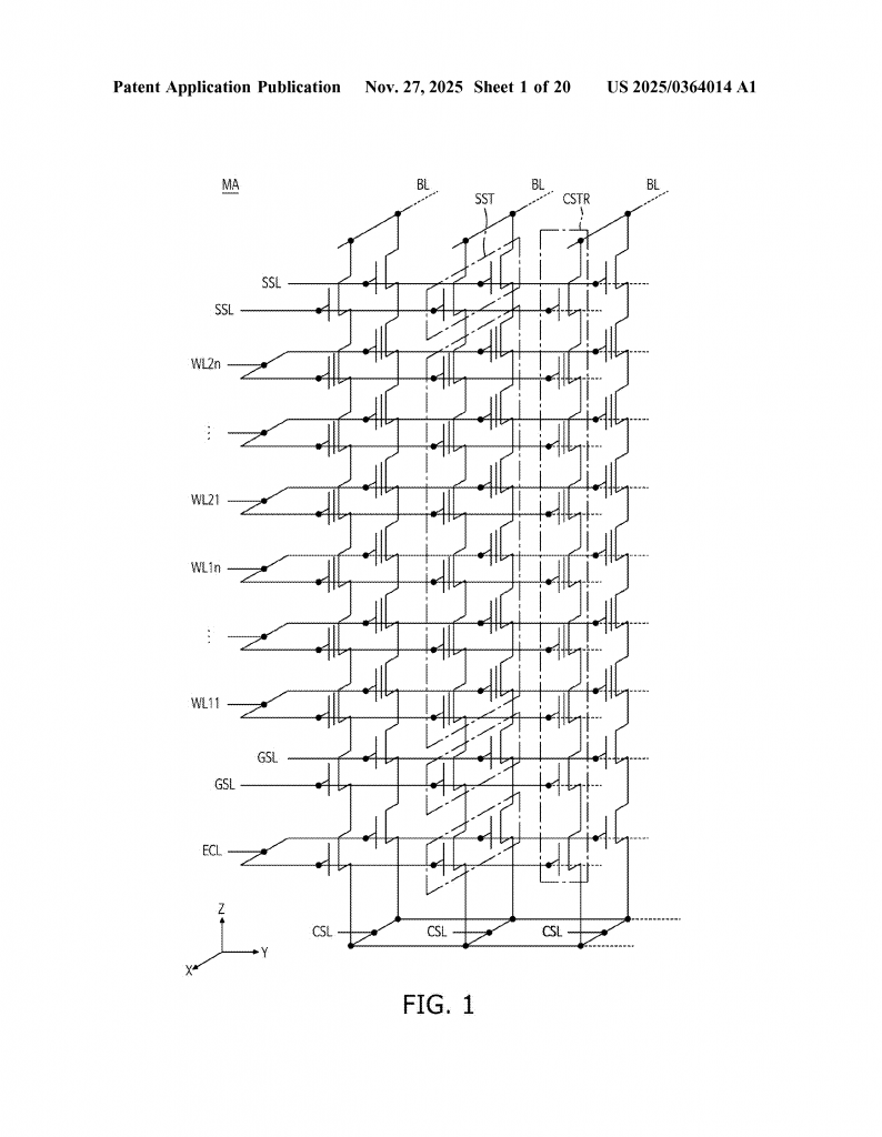
To fully understand the new invention, let’s first talk about how memory chips work and what has already been tried. At the core of these chips are memory cells, small electrical switches that can hold a “1” or a “0.” These cells are arranged in rows and columns, and each row is controlled by a “word line,” while each column is controlled by a “bit line.”
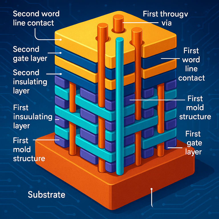
In older memory chips, all these word lines were laid flat on the surface. In 3D memory, word lines are stacked in layers, one above the other. This is called a “mold structure,” which is just a stack of alternating layers: some layers are made to carry electricity (gate layers), and others are insulators that block electricity (insulating layers).
To make a memory chip work, you need to connect each word line to outside circuits that control reading and writing. In a 3D chip, these connections must go through the stack, passing through insulators and gate layers to reach their targets. These connections are called “contacts” or “vias.” The challenge is that as you add more layers, these contacts must be placed closer together. If they are too close, making them without damaging the chip becomes very hard.
Several previous inventions have tried to solve this. Some used different materials for the contacts or spacers to keep signals from leaking out. Others tried to change the way the contacts are arranged, spreading them out or making them in a zigzag pattern. Some used “stair-step” arrangements, where each contact only goes partway through the stack, and new contacts are added as you go up. While these ideas helped, they often made the chip more complex, used up more space, or didn’t solve the problem fully.
Another challenge is that during the chip-making process, tiny masks are used to define where each contact goes. If contacts are too close, the masks wear out faster, or the materials get etched away too much, leading to defects or failed chips. This limits how close contacts can be placed, which in turn limits how dense the memory chip can be.
The new patent builds on these earlier efforts by introducing a way to place contacts and vias even closer together, while keeping the manufacturing process reliable and the chip’s operation safe.
Invention Description and Key Innovations
Now, let’s look at what the new invention does differently and why it matters.
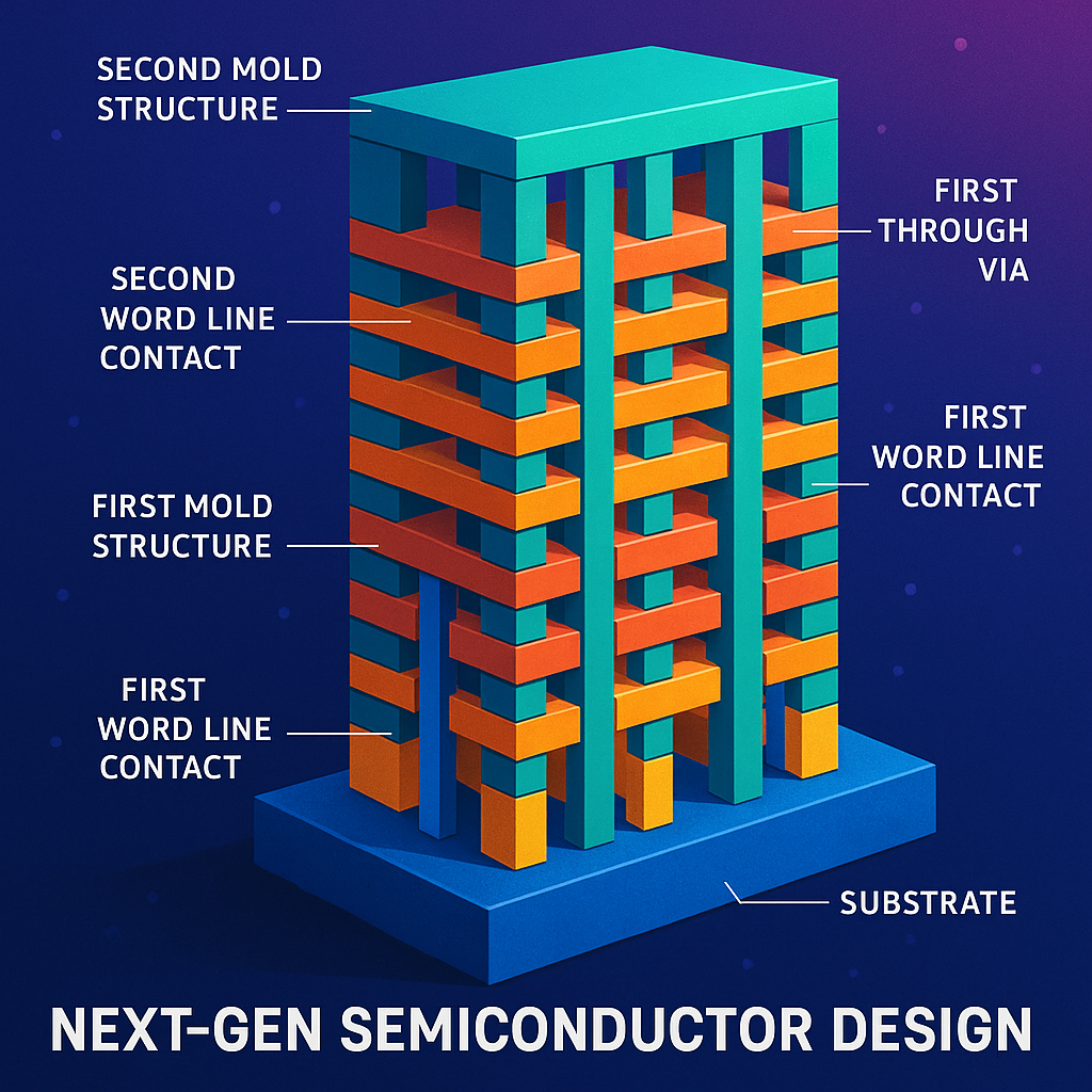
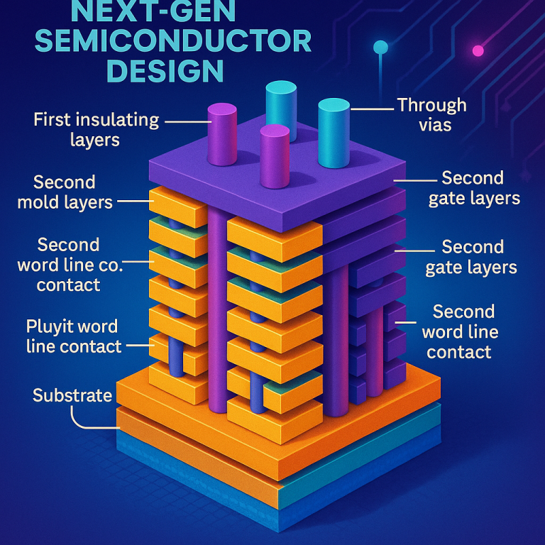
At the heart of this invention is a special way of stacking and connecting the layers inside a semiconductor memory chip. The chip is built on a base called a substrate. On top of this, multiple “mold structures” are stacked. Each mold structure has a repeating pattern: one layer that lets electricity flow (a gate layer), then one that blocks it (an insulating layer), and so on.
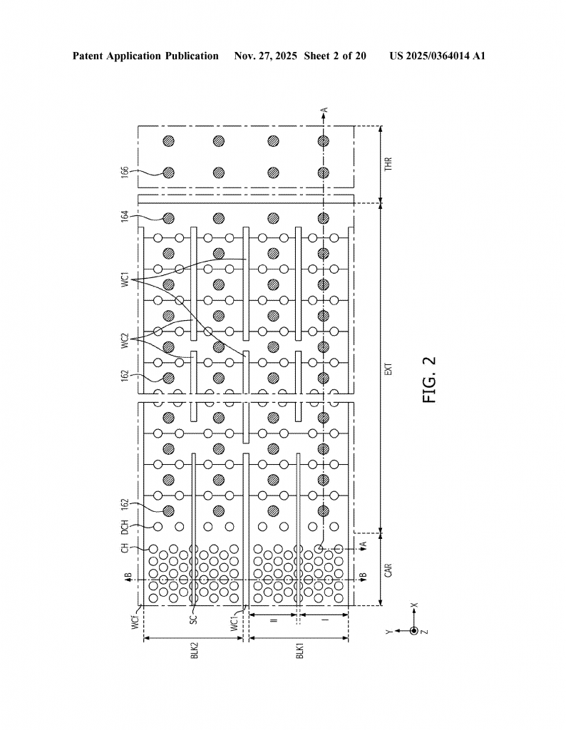
Here’s where the breakthrough happens: Instead of just connecting each word line directly through all the layers, the chip uses a clever combination of contacts and “through vias.” There are two main types of contacts—let’s call them “first word line contacts” and “second word line contacts.” The first word line contacts go through the first mold structure and connect to the first set of gate layers. The second word line contacts go through a second mold structure stacked on top and connect to the next set of gate layers.
But the real magic is in the “through vias.” These are special vertical connections that go through the second mold structure and link back down to the first word line contacts. This setup allows the chip to place the contacts closer together than before, because the vias and contacts are arranged in an alternating, honeycomb-like pattern. This pattern makes better use of space, so more connections fit in the same area without risk of short circuits or manufacturing problems.
In some versions, a third mold structure can be added on top, with its own set of word line contacts and vias. The same alternating arrangement is used, now with three types of contacts and vias interleaved. This means even more layers, and thus more memory cells, can be stacked in a single chip.
The patent also introduces special “spacers”—thin insulating barriers that surround the contacts and vias at certain points. These spacers serve a double purpose: they keep the electrical signals from leaking between layers and protect the contacts during the chip-building process. Some spacers are formed as single layers, while others are made of several layers for extra protection. In some cases, the spacers even cover the bottom and sides of the contacts, like a protective shell.
Another innovation is in the shape of the contacts. In some cases, the diameter of a contact gets smaller as it goes down through the layers. This “tapered” shape helps the manufacturing process and saves space. Some contacts also have tiny voids or empty spaces inside, which makes them easier to make and cools the chip during use.
The patent describes how these new contacts and vias can be made reliably. It explains different steps for stacking layers, adding spacers, etching away materials, and filling in conductive metals. For example, special “sacrificial” films are used during the process and later removed, leaving behind clean holes that can be filled with metal.
Beyond just the chip itself, the patent covers how these chips can be combined into larger electronic systems. Multiple chips can be packaged together, connected by wires or advanced structures called “through silicon vias” (TSVs). The chips can then be mounted on a board alongside controllers and other memory types, like DRAM, to create powerful storage devices for computers, phones, or even cars.
What makes this invention stand out is its ability to pack more memory into less space, while making the manufacturing process easier and more reliable. The alternating, honeycomb arrangement of contacts and vias, the use of layered spacers, and the smart shaping of contacts all work together to achieve higher memory density, lower risk of defects, and better performance.
For anyone in the memory chip industry, this patent points the way to building the next generation of high-capacity, high-speed, and low-cost memory devices. As data needs keep rising, these kinds of advances will be key to keeping our digital world running smoothly.
Conclusion
This new patent shows how clever engineering can keep pushing the limits of what memory chips can do. By rethinking how to connect the many layers inside a 3D memory chip, the inventors have found a way to pack more data into the same space, improve reliability, and keep manufacturing costs down. As the electronics world continues to demand more from memory, these kinds of innovations will shape the future of technology. Whether you are a chip designer, a tech business leader, or just someone curious about how your gadgets work, this invention is an exciting glimpse into what comes next in the world of memory chips.
Click here https://ppubs.uspto.gov/pubwebapp/ and search 20250364014.