Next-Gen Display Manufacturing Boosts Device Performance and Durability for Consumer Electronics
Invented by KO; Seung Cheol, LEE; Young Suk
Display technology continues to shape our lives, from the screens in our pockets to immersive virtual reality glasses. As these devices become smaller, thinner, and sharper, even the smallest manufacturing flaw can cause big headaches—causing dead pixels, lines, or flickers. Today, let’s explore a new patent application that aims to solve a key problem in display manufacturing: stopping pattern defects in the layers that carry electricity through these screens. We’ll break down the market context, examine the scientific thinking and prior art, and then explain the invention’s clever new approach in plain, simple language.
Background and Market Context
If you look around, you’ll see screens everywhere—phones, TVs, watches, laptops, billboards, even inside cars and on refrigerators. These displays are getting clearer, brighter, and more energy efficient every year. The latest trends are all about ultra-high resolution (think tiny pixels packed tightly together), thinner panels, and flexible or foldable screens that can bend or roll up. In addition, new industries like virtual reality (VR) and augmented reality (AR) rely on screens that sit right in front of your eyes, making image quality and reliability even more important.
What most people don’t see, though, is the complex “sandwich” of layers inside every display. There are layers that carry electrical signals (called conductive layers), layers that keep these signals from touching each other (called insulating layers), and layers that actually create the image (like light-emitting diodes or tiny quantum dots). Each layer must be made with great care, and even a small bump or gap in one layer can cause a visible defect in the final product.
In high-resolution displays, where each pixel is tiny and the wiring is very close together, the problem gets harder. The physical “steps” or bumps formed by stacking different patterns of wires or electrodes can make it tough to lay down new layers on top. If the top layer is too thin over a bump, it might break. If it’s too thick, it could cause a short circuit. Either way, you end up with dead pixels or flickering lines—and lots of wasted screens that never make it to market.
Manufacturers have tried to fix this by polishing layers flat or by using different materials, but those methods have problems too. Polishing can introduce dust or even grind away too much material, causing new defects. Using new materials can be costly or hard to control. So, the market is hungry for a better way to create smooth, reliable layers—especially as screens get even sharper and smaller.
This is where the new patent application comes in. It aims to solve these problems by introducing a new way to shape the insulating layer that sits between wiring patterns, using careful etching to create grooves where needed. The goal: make the layers flat enough for reliable wiring, but thick enough to prevent shorts. If it works, it could lead to better screens for phones, TVs, VR glasses, and much more.
Scientific Rationale and Prior Art
Let’s zoom in on the science behind the problem. In every display device, electric signals travel through tiny wires or electrodes to tell each pixel what to do. These conductive layers are patterned—meaning, they aren’t flat sheets, but instead have lines and shapes that form the circuitry. On top of these patterns, you need an insulating layer—think of it as a gentle blanket that keeps the electricity from jumping to the wrong place.
The challenge is that the patterned wires below make the insulating layer uneven. Imagine spreading a blanket over a bunch of pencils and erasers; you get bumps and dips. If you then try to lay another set of wires on top, these bumps can cause the new wires to break (if the layer is too thin over a bump) or lead to unwanted connections if the layer is too thin between wires. These problems are called pattern defects, and they can ruin the whole display.
Historically, manufacturers tried several approaches:
– Chemical Mechanical Polishing (CMP): This is like sanding the blanket flat after you lay it down. It can work, but is risky. Polishing can introduce dust, leave scratches, or remove too much material, thinning the insulation and creating new problems.
– Thicker Insulating Layers: Some tried making the insulating layer extra thick to cover bumps. But this can make it hard to manufacture fine, tightly-packed circuits, leading to bigger, less efficient screens.
– Different Materials: Using combinations of materials with different properties, like putting a soft layer over a hard one, can help a bit. But this can make the process more complicated and costly, and sometimes the materials don’t stick well together.
– Advanced Photolithography: Some companies used more advanced light-based patterning to make layers more even, but this technology is expensive and still struggles with the smallest features.
Even with all these methods, there’s still a big risk of defects—especially as screens get sharper and the wiring gets more crowded. In the best case, you end up with expensive manufacturing steps and lots of wasted materials. In the worst case, you get visible defects right in the middle of your screen. The industry needed a new way to make these insulating layers both flat and reliable, while keeping the process simple and cost-effective.
The inventors behind this patent realized that the key is not to make the whole layer thick or thin, but to make the thickness just right—thin enough over the bumps to keep things flat, but thick enough everywhere else to prevent shorts. This led them to develop a process where they use a careful etching step, guided by a special mask, to create grooves or thinner areas in the insulating layer exactly where needed. By doing this, they can control the flatness and thickness very precisely, allowing the next layer of wiring to be laid down smoothly and reliably.
This approach builds on what came before—like using different materials or etching processes—but adds a new level of control and precision. It avoids the risks of polishing and the cost of exotic materials, and is well-suited for modern, high-density display circuits. The result could be a big leap forward in screen reliability and manufacturing yield.
Invention Description and Key Innovations
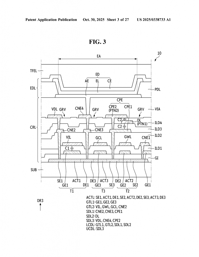
Let’s dig into what’s actually new here—and how it works in practice. The invention is all about the layers inside a display device, especially the circuit layer where all the action happens.
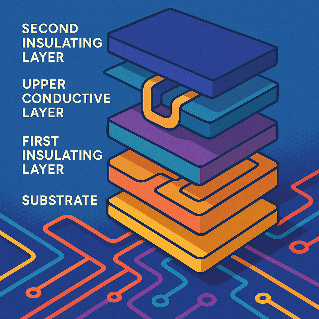
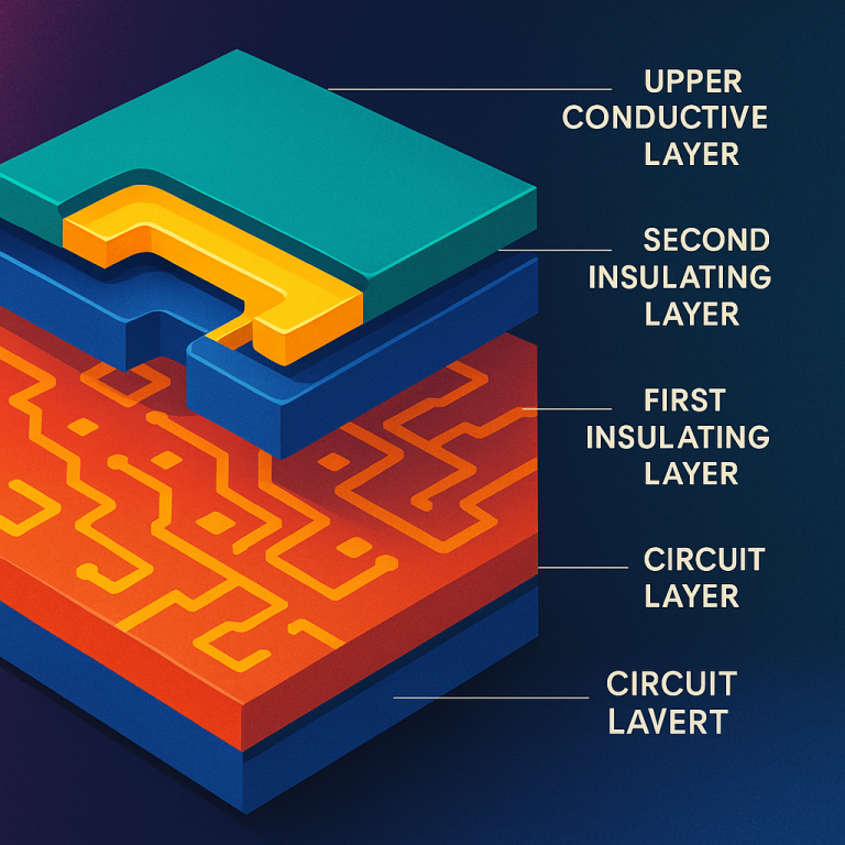
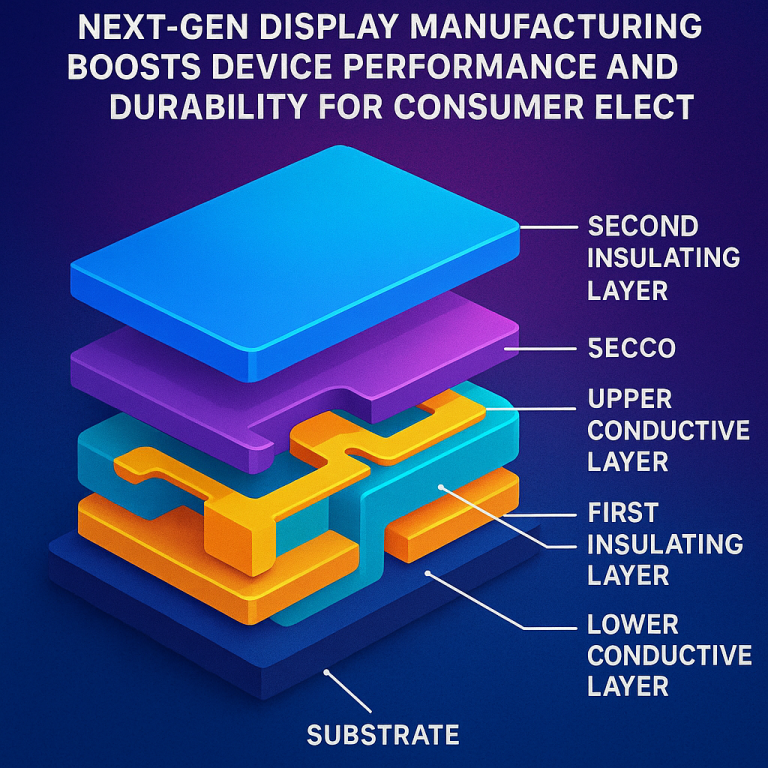
The core structure starts with a substrate—this is the base, like the glass or plastic sheet that forms the bottom of your screen. On top of this, there’s a circuit layer with tiny wires and circuit elements. These wires are made from a lower conductive layer (think of this as the first set of wiring), which includes particular patterns for things like data lines.

Next comes the magic: the first insulating layer. This layer goes on top of the lower wires to keep electricity from jumping where it shouldn’t. But, as we learned above, laying this layer on top of bumpy wiring can create trouble. Here’s where the invention shines.
Instead of making the whole insulating layer thick or thin, the inventors use a mask and etching process to create a groove (a thin spot) in the insulating layer exactly above the bumpiest part of the wiring. The groove is made by carefully etching away just enough material, usually between 200 and 800 angstroms deep (that’s really thin!), so the top of the insulating layer is flatter. This groove is only in the area right above the big bumps—the rest of the layer stays thicker.
On top of this newly flattened insulating layer, the inventors lay down the upper conductive layer—the next set of wires or electrodes. Because the surface is now much flatter, these wires can be patterned without risk of breaking or shorting out. There’s also a second insulating layer on top, adding another level of protection. In some forms, a light-emitting element (like an OLED or micro-LED) is added above all these layers, forming the actual picture-producing part of the display.
The patent also covers more advanced versions, like using multiple insulating layers made from different materials (for example, a layer of silicon nitride under a layer of silicon oxide). In these cases, only the top insulating layer is etched away above the bump, using the different materials’ etch properties to stop the process at just the right point. This lets manufacturers fine-tune the thickness and flatness even more, and gives extra protection to the lower wiring.
The real innovation is in the method of making these layers. By using a mask (a pattern made using photoresist, like in photography), manufacturers can target the etching only at the problem spots. They use dry etching—a process using gases or plasma instead of liquids—to remove just the right amount of material. This is much cleaner and more controlled than old polishing methods, reducing dust and the risk of over-thinning.
The process can be repeated for different layers, and the groove depth and thickness can be controlled to match the needs of the circuit. For example, the thin spot in the insulating layer can be set to just the right size to prevent shorts but allow the upper wires to be made without defects. The patent also describes how this method can be used with different types of displays—OLED, quantum dot, micro-LED, and more.
In short, the key innovations are:
– Using selective etching to make grooves in the insulating layer only where needed, making the surface flatter for later wiring.
– Combining single or multiple insulating materials, so the etching can be carefully stopped at the right depth.
– Avoiding risky polishing steps or excessive thickness, making the process more reliable and suitable for high-density, high-resolution displays.
– Providing a method that can be adjusted for different types of screens and different wiring patterns, making it very flexible for manufacturers.
By putting all these ideas together, the new display device is less likely to have dead pixels or lines, is easier to manufacture with fewer wasted parts, and can be used in the newest, highest-resolution technologies—from smartphones to VR glasses.
Conclusion
Display devices keep advancing, but the challenges of making them reliable and defect-free are more important than ever—especially as screens get smaller, thinner, and more tightly packed with circuits. The patent application we’ve explored today offers a smart, tactical approach: instead of trying to make every layer perfect everywhere, it focuses on fixing only the problem spots, using precise etching to flatten the insulating layer in just the right places. This makes the next wiring layer easier to lay down, reduces the risk of defects, and keeps screens bright and clear.
For anyone in the display manufacturing world, this invention could be a game-changer—reducing costs, improving yield, and supporting the next generation of ultra-sharp, flexible, or wearable screens. For consumers, it means fewer dead pixels, longer-lasting devices, and better experiences—whether you’re watching a movie, playing a game, or exploring a virtual world. As the demand for better displays continues to grow, smart solutions like this will keep us all looking forward to what’s next.
Click here https://ppubs.uspto.gov/pubwebapp/ and search 20250338733.