New Manufacturing Method Boosts Efficiency and Performance in Next-Gen Display Devices
Invented by UM; Jae Gwang, LEE; Tae Hee, CHANG; Moon Won, Samsung Display Co., LTD.
Understanding a New Way to Make Display Devices: A Deep Dive into a Recent Patent Application
Making screens for phones, TVs, and other devices takes clever ideas. A new patent application shows a fresh method to build these display devices, hoping to make them more reliable. Let’s break down what this patent covers, why it matters, and how it works, all in clear and simple words.
Background and Market Context
Screens are everywhere. Look around and you will see phones, watches, tablets, smart glasses, and car dashboards — all using displays. People want these screens to be bright, sharp, and last a long time. They also want them in new shapes, like curved or foldable screens. But making these screens is tricky, especially when putting tiny light pieces (called light emitting elements) onto the main part of the screen, or substrate.
As screens get smarter and smaller, companies are looking for better ways to make them. Firms are racing to find ways to build displays that use less power, show more colors, and can bend or fold. This is especially important for new technology, like smartwatches, cars, and virtual reality headsets. If even one tiny light part doesn’t stick well or breaks during making, it can ruin the whole screen. That’s why reliability — making sure each tiny part works and stays in place — is so important.
The old way to build screens meant picking up and moving each little light part, like picking up grains of rice one by one with tweezers. This could cause problems. Sometimes the part would not stick, or it would break. Sometimes, the process would leave behind glue or dirt, making the screen less clear. Companies spent a lot of time and money on fixes. As the demand for thinner, lighter, and bendable screens grows, the need for a new way becomes even stronger.
The new patent we are looking at tries to solve these problems. It offers a method to make screens in a way that is easier, cleaner, and more reliable. If this method works well, it could help companies make better screens faster and with less waste. This could mean better products for everyone, from phones that last longer to smart glasses that are more comfortable to wear.
Scientific Rationale and Prior Art
To understand the new idea, let’s look at how screens are made now. Each display has lots of tiny lights called pixels. Each pixel is made from light emitting elements, like tiny LEDs or OLEDs. These are made on one surface (called the growth substrate), then moved to the main surface (the display substrate) where they light up to show pictures.
The problem is moving these tiny light parts without breaking them. The old ways used glue or sticky tape to pick up each part, move it, and stick it down. Sometimes, lasers were used to cut or move the parts. These steps could damage the parts or leave behind unwanted stuff. If a light part didn’t stick well, the screen would have dark spots or might not work at all.
Other patents tried to fix this by using special tools or by changing the glue. Some used lasers to help move the parts. A few tried to use metal pads or bumps to stick parts together, but these could still break or not join well. The main problem was making sure the bond — the connection — between each light part and the main screen was just right: not too weak, not too strong, and very clean.
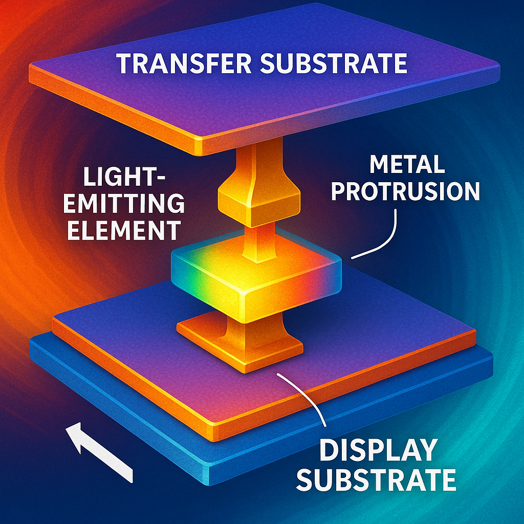
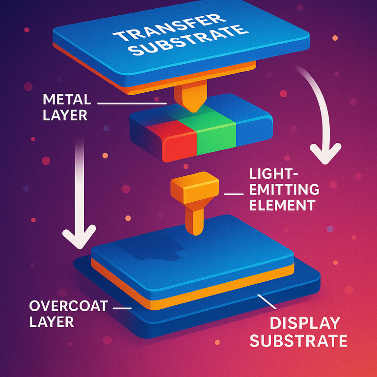
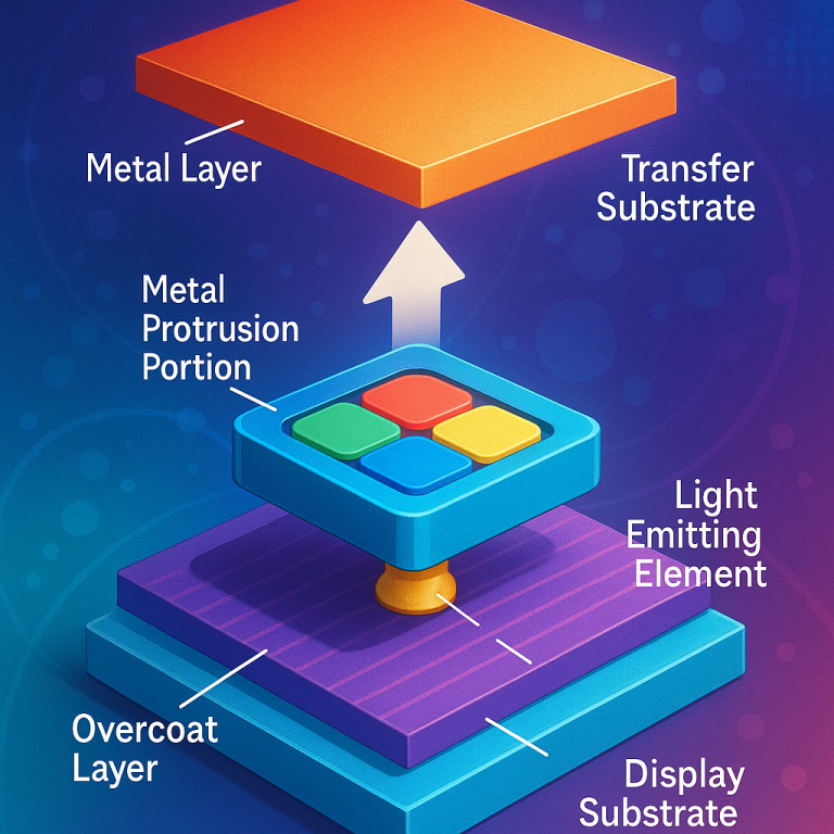
The new patent takes a different path. It uses a “transfer substrate” with a metal layer. The tiny light part (the light emitting element) has a “metal protrusion,” like a little metal bump or peg. This metal peg is first joined to the transfer substrate’s metal layer. This is done by heating, sometimes with a laser, so the two metals partly melt together (called “alloying”). This holds the light part tightly to the transfer substrate.
Next, the transfer substrate is lined up with the main screen (the display substrate). The light part is gently pushed onto the screen’s “overcoat layer,” which may have glue or a sticky material. The bond between the light part and the overcoat is made to be stronger than the bond between the metal peg and the light part. When the transfer substrate is pulled away, the metal peg pulls free from the light part and stays behind, still stuck to the transfer substrate. The light part stays stuck on the screen where it belongs.

This clever way means the light part can be placed just right and won’t move. The method also lets the metal peg be reused, or at least stops it from getting in the way. There’s less dirt, less damage, and less chance of problems. The process can be done in steps for lots of light parts at once, which saves time.
What’s new here is the use of a metal peg that is only meant to help in moving the light part, and then is removed. The careful control of how strong each connection is — peg to substrate, peg to light part, light part to screen — is also new. The process uses lasers and heating in a controlled way to join and separate the parts without hurting them.
Most past patents focused on sticking the light part for good with glue or direct metal-to-metal bonds. Few thought of using a “sacrificial” metal peg that is bonded, then removed in a controlled way by making sure the right bonds are stronger than others. This is the key difference of the new patent.
Invention Description and Key Innovations
Now, let’s talk about the heart of the patent. The invention is a step-by-step way to build a display device that solves old problems. Here’s how it works, written simply:
First, the tiny light part (light emitting element) is made on a special starting sheet, called the growth substrate. This part has layers of stuff that make it light up: two semiconductor layers with an “active” layer between them. On the outside, there’s an insulating film to keep it safe. Sticking out from the sides are two bonding electrodes, which connect to power later. On top, there’s a little metal peg that sticks out more than the electrodes.
Next, the transfer substrate, which is just a strong sheet with a metal layer, is lined up so its metal is right above the metal peg of the light part. The two are pressed together and heated, sometimes with a laser. This makes the peg and the metal layer partly melt together (alloy), forming a tight, but not permanent, bond. The light part is now stuck to the transfer substrate by the metal peg.
A laser is then used to gently cut the light part free from the growth substrate, without hurting it. Now, the light part is only attached to the transfer substrate by the metal peg.
The transfer substrate is brought close to the main screen, called the display substrate. The display substrate has an overcoat layer, which may be sticky or have glue. The transfer substrate is moved so the light part touches and sticks to the overcoat layer, which is made to grip the light part more tightly than the metal peg does.
The transfer substrate is then pulled away. The bond between the metal peg and the light part is weaker than the bond between the light part and the overcoat. This means the metal peg pulls away and stays stuck to the transfer substrate, while the light part remains in place on the display substrate. This is possible because the patent carefully controls the strength of all the bonds: peg to light part, peg to transfer substrate, and light part to screen.
After this, more parts can be added to finish the screen, like electrodes, protective layers, or color filters. The process can be repeated many times, placing each tiny light part where it belongs, quickly and accurately.
The patent also allows for different shapes and arrangements of the metal peg. Sometimes there may be two pegs, each lining up with a different electrode. The method can use lasers for heating, or it can use other ways to make the metals bond.
The big ideas here are:
1. A sacrificial metal peg: It helps move the light part and is then removed, which keeps things clean and simple.
2. Controlled bond strengths: By making sure each bond is just the right strength, the parts separate and stay in place without breaking.
3. Laser-assisted bonding and cutting: Using lasers means less damage to the parts and more accuracy.
4. Scalability: The method can be used to place many light parts at once, instead of one by one, which saves time.
This process can help make screens that are thinner, last longer, and have fewer broken parts. It can also be used for many types of screens, from small smartwatches to big TVs, and for new shapes like curved or bendable displays.
Most importantly, this way is gentler on the tiny light parts. It keeps them clean, safe, and exactly where they need to be, which means better screens for everyone.
Conclusion
This new patent shows a smart way to make screens by using a metal peg to help move and place tiny light parts. By carefully controlling how strong each connection is, and by using lasers to bond and separate parts, the process becomes more reliable and makes better screens. If this method is used, we can expect brighter, longer-lasting, and more flexible displays in the future. The screens in your next phone, watch, or car might use this very method, helping bring sharper images and new shapes to life.
Click here https://ppubs.uspto.gov/pubwebapp/ and search 20250218848.