CONTAMINATION PREVENTION DEVICE FOR EXTREME ULTRA-VIOLET (EUV) RETICLE AND EUV EXPOSURE APPARATUS INCLUDING THE SAME
Invented by KIM; Hoonseop, NAM; Sangki, JANG; Sungho, MUN; Jehoi, YOO; Nali, LEE; Changwook, SAMSUNG ELECTRONICS CO., LTD.
Keeping semiconductor manufacturing clean is a huge challenge, especially when making chips with extremely small features. This new patent application introduces a smart way to prevent tiny particles from sticking to extreme ultraviolet (EUV) reticles, which are key parts of the machines that print tiny patterns on chips. Let’s break down the problem, the science behind it, and the clever solution that’s being proposed.
Background and Market Context
Every year, our phones, computers, and cars get faster and smarter. This progress is powered by microchips made with smaller and smaller features. To print such tiny features, chip makers use a process called photolithography, which shines light through or off of a patterned mask (called a reticle) to copy the pattern onto a wafer. For the smallest features, the industry uses extreme ultraviolet (EUV) light, which has a much shorter wavelength than older light sources. This shorter wavelength lets factories print very small features, but it also brings a whole new set of challenges.
In older photolithography machines, masks were protected by a thin membrane called a pellicle, which caught dust and kept the mask clean. But EUV light is so powerful that it quickly damages any pellicle, so EUV reticles are left exposed. This means that any tiny particle in the air can land on the reticle and ruin a chip, sometimes ruining an entire batch. Even the smallest speck can create a flaw in the chip below. Because each reticle is used to print patterns onto many wafers, a single dirty reticle can cause massive losses and disrupt production lines.
As chips become more complex and the cost of manufacturing keeps rising, the need to prevent contamination gets even more urgent. Factories invest millions in clean rooms and air filters, but some particles always sneak through. EUV reticles are especially sensitive because of the way they work: instead of letting light pass through, they reflect EUV light using a stack of special materials. This stack can easily collect static electricity and attract charged particles, making the contamination problem worse. The industry is desperate for a solution that keeps EUV reticles clean, without blocking the EUV light or slowing down production.
Scientific Rationale and Prior Art
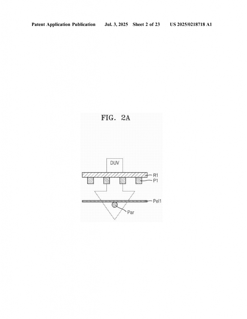
The science behind EUV contamination is both simple and tricky. In EUV machines, the reticle is bombarded with very high-energy light. This light can knock electrons out of the reticle’s surface in a process called the photoelectric effect. When electrons are lost, the reticle’s surface becomes positively charged. At the same time, the air around the reticle contains hydrogen gas, which is needed to keep things clean. The EUV light turns some of this hydrogen gas into plasma, which is made up of free electrons and ions.
Some of the free electrons from the plasma can neutralize the positive charge on the reticle, but not enough. Most of these electrons end up sticking to tiny particles floating in the air, giving those particles a negative charge. Now we have a positively charged reticle and negatively charged dust particles. As you might guess, opposites attract. The electric force pulls these particles right onto the reticle, where they stubbornly stick. Once there, they are hard to remove and can damage many wafers before anyone notices.
Older solutions focused on physical barriers, like pellicles, but these don’t work with EUV. Other ideas included blowing air or gas to move particles away or using special coatings that repel dirt. Some machines even tried to neutralize the static charge on the reticle by flooding the area with more plasma or using ionizers. But these methods can be slow, hard to control, or can introduce new problems, such as interfering with the light path or damaging the delicate reticle surface. None of these earlier approaches offered a real-time, precise, and reliable way to keep the reticle neutral and free of static buildup, especially during the actual exposure process.
Another issue with older approaches is that they often treated all particles the same. But tiny particles, especially those less than 100 nanometers wide (that’s about a thousand times thinner than a human hair), are most affected by electric forces and are the hardest to control. The smaller the particle, the stronger the electric pull toward the charged reticle. Once these small particles stick, they are very hard to get rid of, even with air jets or cleaning cycles.
This is the scientific challenge: how can we keep the reticle neutral and stop particles from sticking, right during exposure, without getting in the way of the light or slowing down the process?
Invention Description and Key Innovations
The patent application introduces a smart and flexible device that keeps the reticle neutral by using electron sources and sensors. Here’s how it works, in plain language:
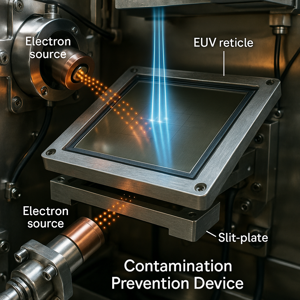
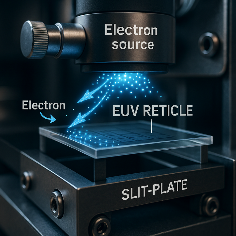
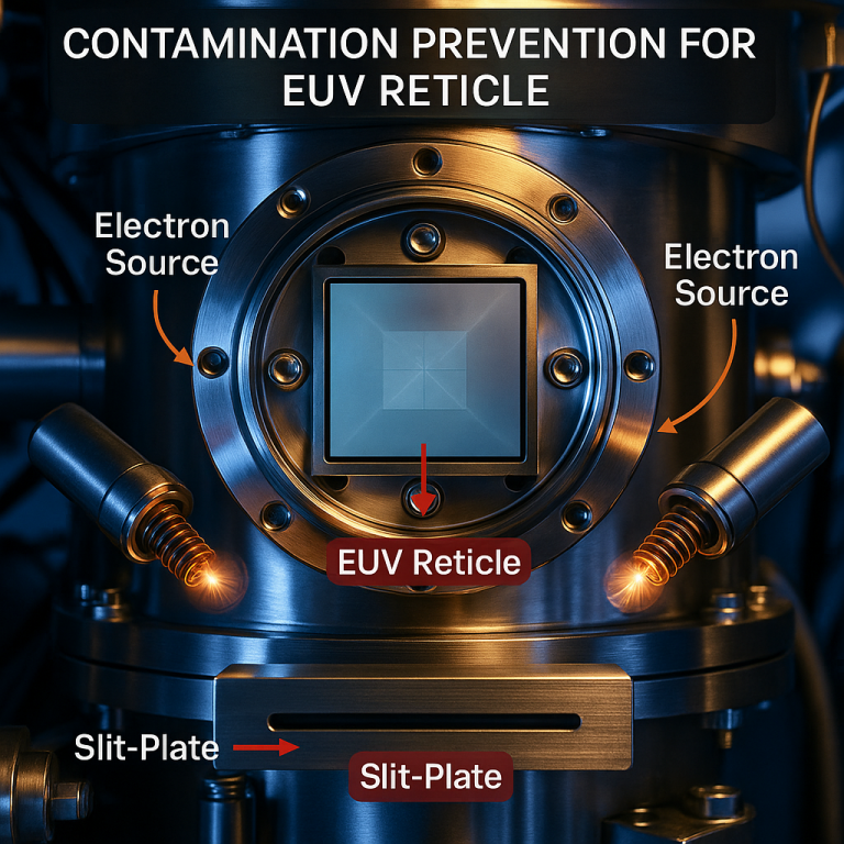
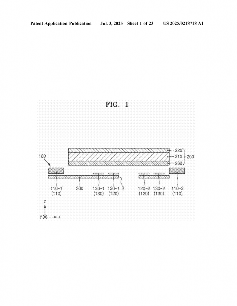
Imagine the reticle sitting above a thin metal plate with a slit (the slit-plate), where the EUV light shines through. On each side of the reticle, just outside the space between the reticle and the slit-plate, the device places one or more electron sources. These can be electron guns or other devices that shoot out electrons when needed. The job of these electron sources is to send electrons into the space between the reticle and the slit-plate, right where the light hits and where particles might sneak in.
To decide when and how much to fire, the device uses two types of sensors:
First, plasma sensors are placed near the slit opening. These detect whether plasma (from the hydrogen gas turning into charged particles) is present. If plasma is found, it means there are already some free electrons in the area, which can help neutralize the reticle. But if there is no plasma, the device knows it may need to step in and add electrons.
Second, surface charge sensors are also placed near the slit. These watch the reticle’s surface to see if it is building up a positive charge. If the reticle gets too positive, it’s at risk of pulling in negative particles.
Based on what the sensors find, the electron sources can respond in several smart ways:
If the sensors show no plasma and the reticle is charged, the electron sources turn on and shoot electrons into the space, aiming to neutralize the positive charge. This can be done by firing from one side first and then the other, both at once, or in a timed sequence, depending on what works best for the setup. This flexibility allows for fast, even neutralization across the whole reticle surface, no matter the scanning direction of the exposure process.
By keeping the reticle’s charge close to zero (neutral), the electric pull that would otherwise attract dust is blocked. Particles in the air are no longer drawn to the reticle, and if they do land nearby, they don’t stick and can be easily blown away in the next cleaning step.
This approach is unique because it acts in real time, right during the exposure process. The sensors make sure the system responds only when needed, so it doesn’t waste energy or risk over-correcting. The electron sources are placed outside the critical light path, so they don’t interfere with the EUV light or the patterning process. The whole system can be tuned for different scanning directions, reticle sizes, or exposure speeds, making it adaptable for various machine designs.
In addition, the device can work with only one electron source if needed, or multiple sources for faster response. The sensors can be electrical or optical, allowing for different ways to measure plasma and surface charge. The result is a smart, flexible, and non-invasive way to keep EUV reticles clean, even as chip features keep shrinking.
Tests and simulations described in the patent show that this method quickly brings the reticle’s surface charge back to neutral, stopping the electric forces that trap dust. Particles no longer rush toward the reticle, and their movement becomes almost random, making them much easier to remove with regular air flows. This means fewer defects, less downtime, and higher yields in the fab.
Conclusion
This new contamination prevention device for EUV reticles is a breakthrough for the chip-making world. By using sensors and electron sources together in a smart feedback loop, it solves the problem of static charge and particle contamination right at the source. The system is gentle, fast, and flexible, fitting into the tight spaces and strict requirements of EUV lithography tools. As chips get smaller and the cost of failure gets higher, smart solutions like this will be key to keeping production lines running and pushing technology forward. If you work in semiconductor manufacturing or are looking to license or adopt leading-edge cleanroom technologies, this patent application is worth a close look.
Click here https://ppubs.uspto.gov/pubwebapp/ and search 20250218718.